Touch panels, method for fabricating touch panels, display devices, and method for fabricating display devices
a touch panel and display device technology, applied in the field of capacitive touch panels, can solve the problems of reducing the quality of display, the gap between adjacent electrodes cannot be 100 m or smaller by screen printing, and the cost of vacuum devices and photo-etching devices, etc., and achieves the effect of less visible, less distinguishable, and less visibl
- Summary
- Abstract
- Description
- Claims
- Application Information
AI Technical Summary
Benefits of technology
Problems solved by technology
Method used
Image

Examples
first embodiment
Advantages of First Embodiment
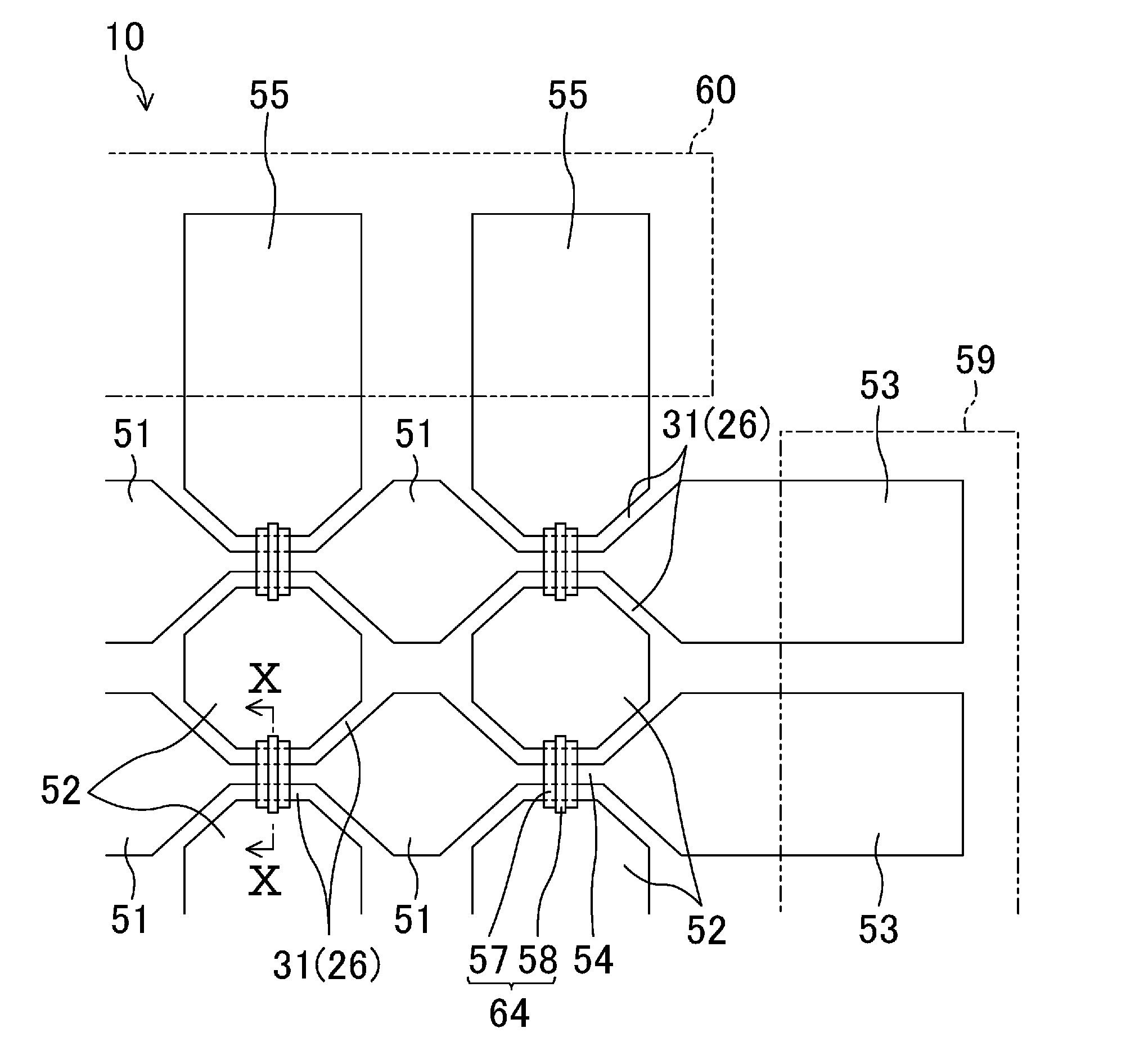
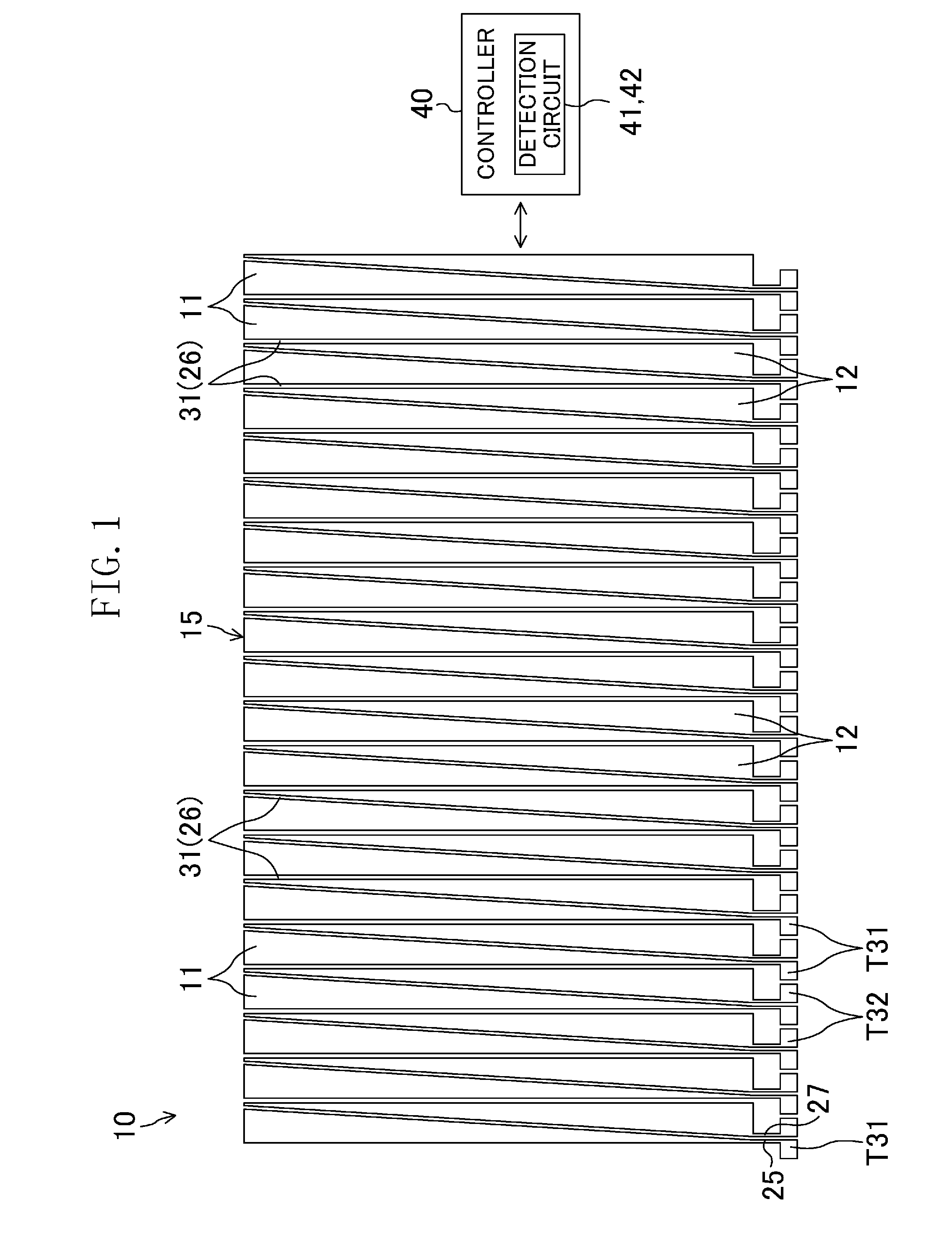
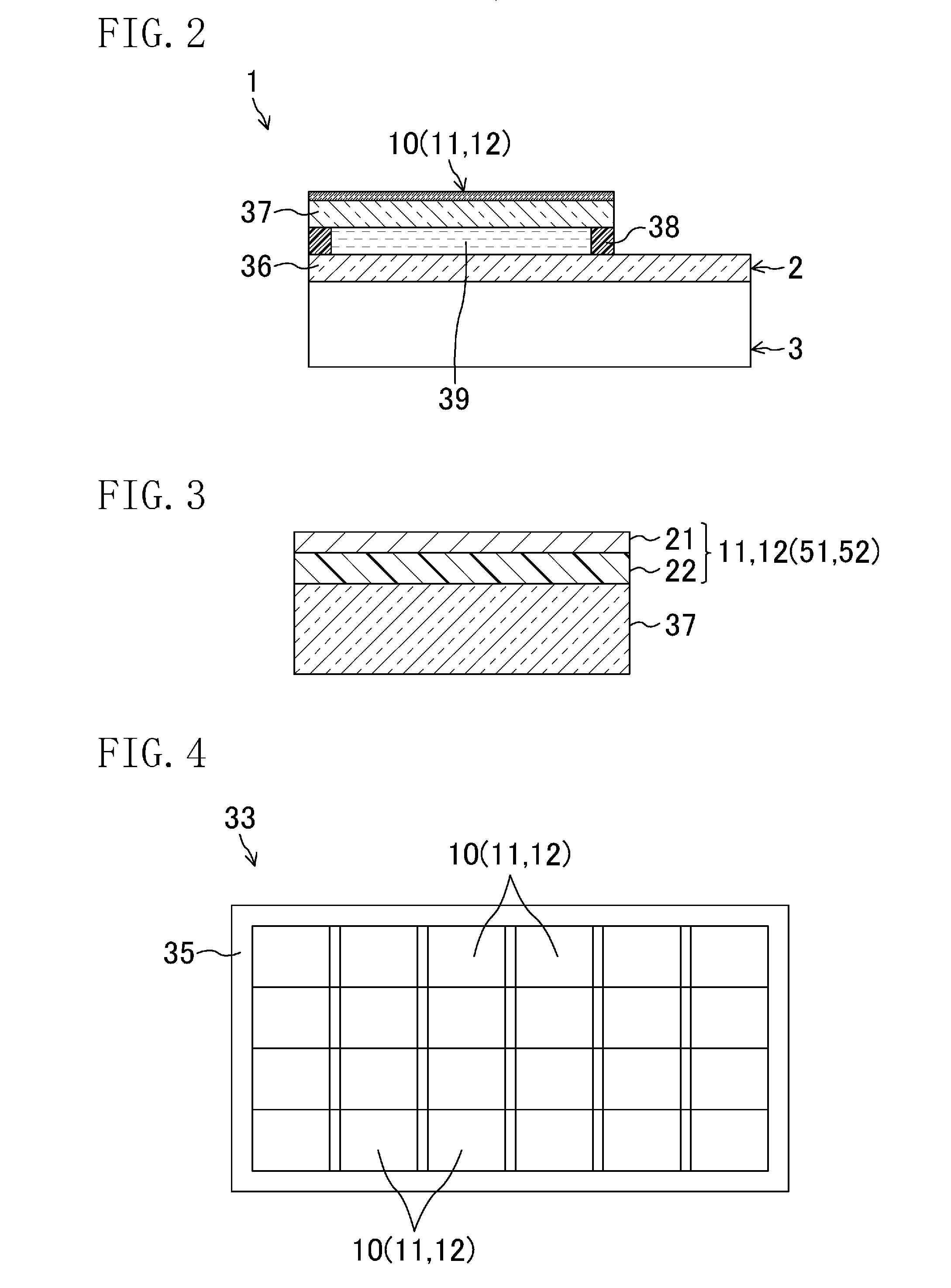
[0097]According to the first embodiment, the first and second electrodes 11 and 12, which are the touch location detection electrodes 11, 12, are formed with the conductive film including the transparent conductive layer 21, and the adhesive layer 22 stacked on the transparent conductive layer 21. Thus, the first and second electrodes 11 and 12 can easily be formed by processing the conductive film adhered to the substrate 35 by a laser.
[0098]Further, the refractive index of the translucent material 31 provided in the gap 26 between the touch location detection electrodes 11, 12 adjacent to each other is set equal to the refractive index of the adhesive layer 22 or the refractive index of the transparent conductive layer 21 constituting the conductive film, or is set to a median between the refractive indices of the adhesive layer 22 and the transparent conductive layer 21. This can reduce a difference between the refractive index of the gap 26 and the ...
second embodiment
Advantages of Second Embodiment
[0115]According to the second embodiment, the water-repellent translucent material 31 is formed on the substrate 35, and then the water-soluble transparent conductive material is applied thereto. Thus, the transparent conductive material is repelled by the translucent material 31 in the region for forming the gap 26 between the first and second electrodes 11 and 12. This eliminates the step of forming the first and second electrodes 11 and 12 by patterning, and allows easy formation of the first and second electrodes 11 and 12 and the gap 26 in which the transparent material is provided.
[0116]The translucent material 31 having the same light transmittance and color tone as the organic transparent conductive film constituting the first and second electrodes 11 and 12 is provided in the gap 26 between the first and second electrodes 11 and 12 adjacent to each other. This can make the translucent material 31 provided in the gap 26 and the electrodes 11 an...
third embodiment
Advantages of Third Embodiment
[0135]According to the third embodiment, the first and second electrodes 51 and 52 are formed with the conductive film (the ITO transfer film). Thus, the first and second electrodes 51 and 52 can easily be formed by laser processing in the same manner as the first embodiment.
[0136]The refractive index of the translucent material 31 provided in the gap 26 is set equal to the refractive index of the adhesive layer 22 or the refractive index of the transparent conductive layer 21 constituting the conductive film, or is set to a median between the refractive indices of the adhesive layer 22 and the transparent conductive layer 21. This can reduce a difference between the refractive index of the gap 26 and the refractive index of the electrodes 11, 12 surrounding the gap. Thus, in the same manner as the first embodiment, the pattern of the electrodes 51 and 52 can be less visible to the users, thereby improving quality of display on the liquid crystal displa...
PUM
| Property | Measurement | Unit |
|---|---|---|
| Electrical conductor | aaaaa | aaaaa |
| Translucency | aaaaa | aaaaa |
| Transparency | aaaaa | aaaaa |
Abstract
Description
Claims
Application Information
 - R&D
- Intellectual Property
- Life Sciences
- Materials
- Tech Scout
- Unparalleled Data Quality
- Higher Quality Content
- 60% Fewer Hallucinations
Browse by: Latest US Patents, China's latest patents, Technical Efficacy Thesaurus, Application Domain, Technology Topic, Popular Technical Reports.
© 2025 PatSnap. All rights reserved.Legal|Privacy policy|Modern Slavery Act Transparency Statement|Sitemap|About US| Contact US: help@patsnap.com