Data output buffer and memory device

a data output buffer and memory device technology, applied in the field of memory devices, can solve the problems of degrading the integrity of command, address, and/or data signals being communicated unsatisfactory signal reflection on the transmission line, and potential noise sources and conditions have come under renewed scrutiny

Active Publication Date: 2012-04-26
SAMSUNG ELECTRONICS CO LTD
View PDF8 Cites 58 Cited by
  • Summary
  • Abstract
  • Description
  • Claims
  • Application Information

AI Technical Summary

Problems solved by technology

Improperly matched impedances will result in undesirable signal reflections on the transmission line.
Such signal reflections degrade the integrity of command, address, and / or data signals being communicated on the transmission line.
Noise has always been a design problem related to data transmission systems, but as memory systems run at ever increasing speeds, potential noise sources and conditions have come under renewed scrutiny.

Method used


Image

  • Data output buffer and memory device
  • Data output buffer and memory device
  • Data output buffer and memory device

Examples


Embodiment Construction

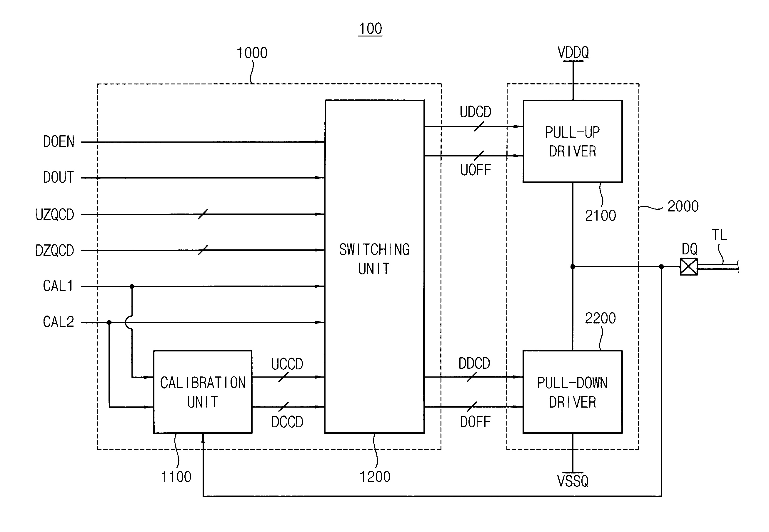
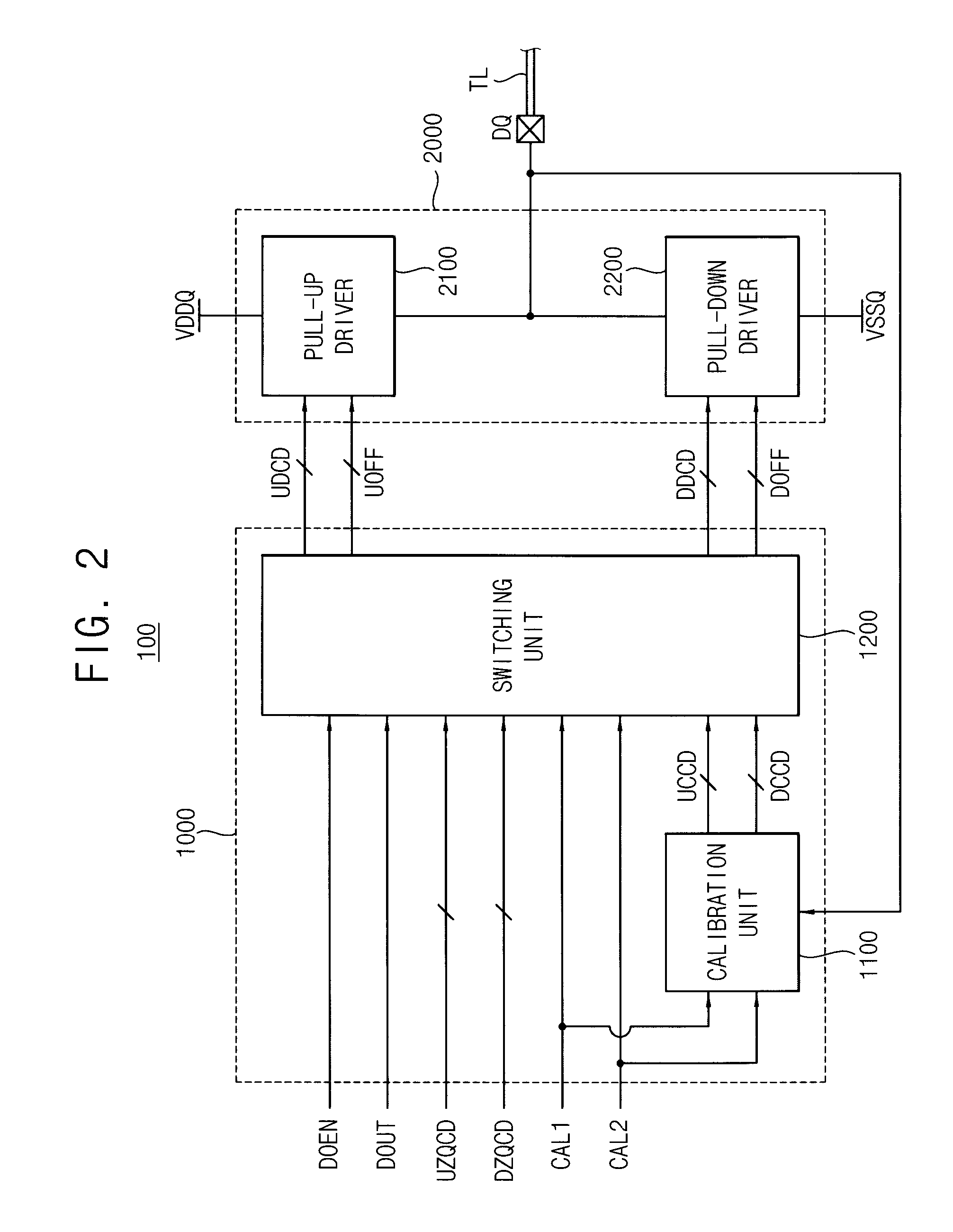
[0027]Certain embodiments of the inventive concept will now be described in some additional detail with reference to the accompanying drawings. The inventive concept may, however, be embodied in many different forms and should not be construed as limited to only the illustrated embodiments. Rather, these embodiments are provided so that this disclosure will be thorough and complete, and will fully convey the scope of the present inventive concept to those skilled in the art. Throughout the written description and drawings, like reference numbers and labels denote like or similar elements.

[0028]It will be understood that, although the terms first, second, etc. may be used herein to describe various elements, these elements should not be limited by these terms. These terms are used to distinguish one element from another. For example, a first element could be termed a second element, and, similarly, a second element could be termed a first element, without departing from the scope of ...


PUM


Abstract

A data output buffer includes a driving unit and a control unit. The driving unit selectively performs a termination operation that provides a termination impedance to a transmission line coupled to an external pin, and a driving operation that provides a drive impedance to the transmission line while outputting read data. The control unit adjusts a value of the termination impedance and a value of the drive impedance based on an output voltage at the external pin during a termination mode, and controls the driving unit to selectively perform one of the termination operation and the driving operation during a driving mode.

Description

CROSS-REFERENCE TO RELATED APPLICATION(S)[0001]This application claims priority under 35 USC §119 to Korean Patent Application No. 10-2010-0102178 filed on Oct. 20, 2010, the subject matter of which is hereby incorporated by reference.BACKGROUND OF THE INVENTION[0002]The inventive concept relates to memory devices, and more particularly to data output buffers and memory devices including the data output buffer.[0003]Careful consideration must be given to the impedance matching between a memory device, or more particularly the input or output buffer of a memory device, and a connected transmission line. Improperly matched impedances will result in undesirable signal reflections on the transmission line. Such signal reflections degrade the integrity of command, address, and / or data signals being communicated on the transmission line.[0004]Noise has always been a design problem related to data transmission systems, but as memory systems run at ever increasing speeds, potential noise so...

Claims


Application Information

Patent Timeline
Patent Type & Authority Applications(United States)
IPC IPC(8): G11C7/00G11C7/10
CPCG11C7/1057G11C2207/2254G11C29/028G11C29/022G11C5/14G11C7/10G11C7/22G11C11/4096H03K19/0005
Inventor KIM, SI-HONGBAE, SEUNG-JUNLEE, JIN-ILPARK, KWANG-IL
Owner SAMSUNG ELECTRONICS CO LTD
Why Eureka
Try Eureka