Method of manufacturing organic light emitting device and method of manufacturing organic light emitting display apparatus using the same

Inactive Publication Date: 2012-04-26
SAMSUNG DISPLAY CO LTD
View PDF5 Cites 2 Cited by
  • Summary
  • Abstract
  • Description
  • Claims
  • Application Information

AI Technical Summary

Benefits of technology

[0036]The method of manufacturing an organic light emitting device and the method of manufacturing an organic light emitting display apparatus may readily increase the characteristics of an intermediate layer having an organic light emitting layer.

Problems solved by technology

For instance, it may be formed by using a deposition method or a thermal transfer method, since an organic material cannot be easily wet patterned.
However, prior to a transfer process using heat, it is difficult to precisely handle the donor film and a substrate on which the transfer process is performed using the donor film, and thus, there is a limit in forming an organic light emitting layer having desired characteristics.

Method used


Image

  • Method of manufacturing organic light emitting device and method of manufacturing organic light emitting display apparatus using the same
  • Method of manufacturing organic light emitting device and method of manufacturing organic light emitting display apparatus using the same
  • Method of manufacturing organic light emitting device and method of manufacturing organic light emitting display apparatus using the same

Examples


Embodiment Construction

[0040]The present invention will now be described more fully with reference to the accompanying drawings in which exemplary embodiments of the invention are shown.

[0041]FIGS. 1 through 10 are cross-sectional views for sequentially illustrating a method of manufacturing an organic light emitting device, according to an embodiment of the present invention.

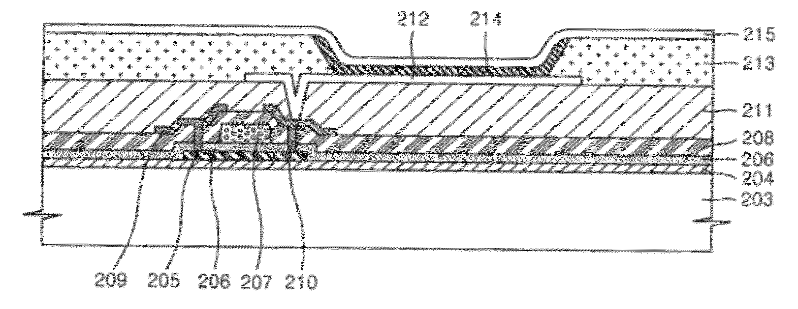
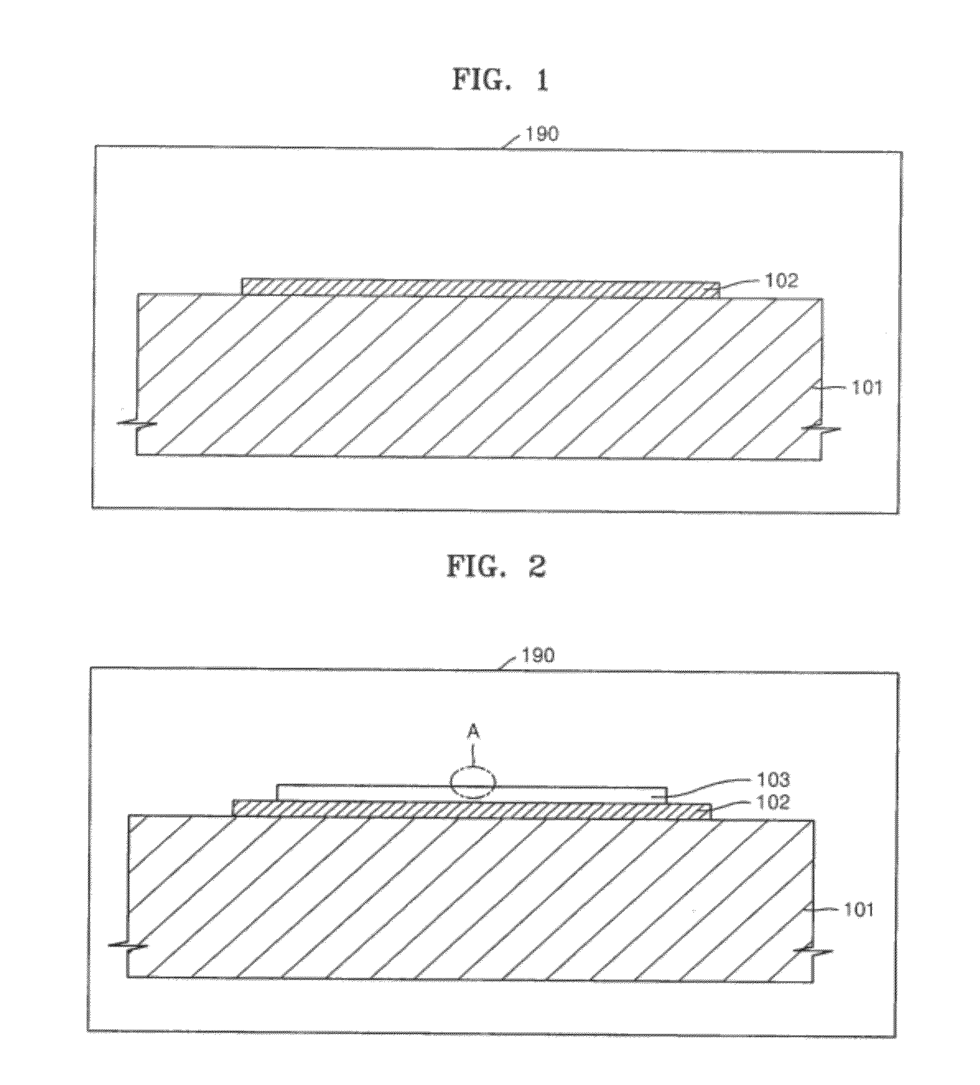
[0042]Referring to FIG. 1, a base member 102 is prepared. The base member 102 may be disposed on a work table 101. The base member 102 and the work table 101 may be disposed in a vacuum chamber 190. Although not shown, the vacuum chamber 190 may easily control the degree of vacuum to a desired level by being connected to a vacuum pump.

[0043]The base member 102 may be a flexible film type member. As a practical example, the base member 102 may be formed, e.g., of a plastic material or a glass material.

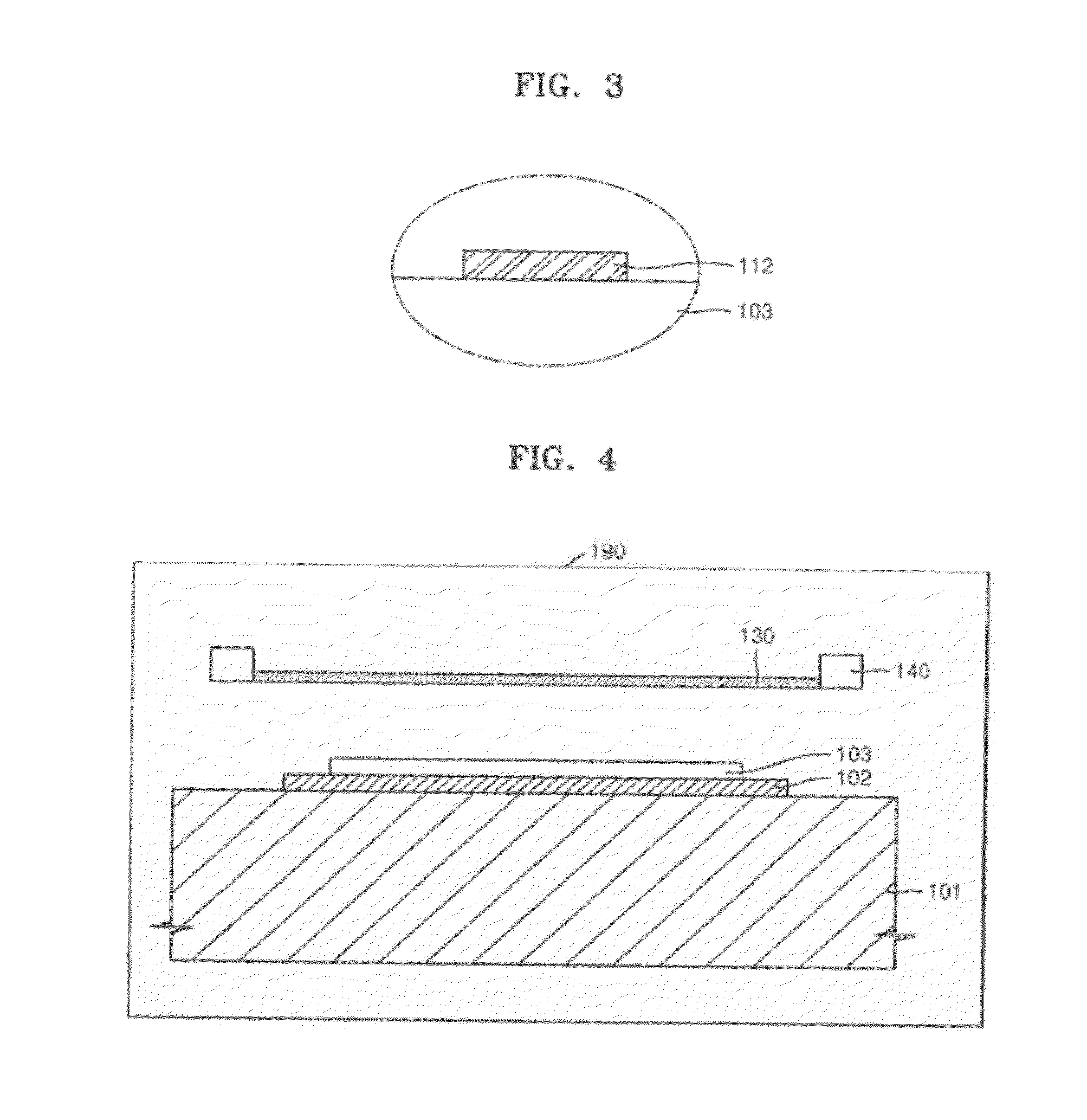
[0044]Referring to FIG. 2, a substrate 103 is disposed on the base member 102. FIG. 3 is a magnified view of portion A of FIG. 2. Refer...


PUM


Abstract

A method of manufacturing an organic light emitting device that readily increases the characteristics of an intermediate layer having an organic light emitting layer, and a method of manufacturing an organic light emitting display apparatus. The method of manufacturing an organic light emitting device includes preparing a substrate having a first electrode; disposing the substrate on a base member; disposing a donor film that covers the substrate and contacts the base member exposed around the substrate; combining the base member and the donor film; forming an intermediate layer having an organic light emitting layer on the first electrode by performing a transfer process in a laser thermal transfer apparatus after placing the base member and the donor film combined with each other with the substrate interposed therebetween in the laser thermal transfer apparatus; and forming a second electrode on the intermediate layer.

Description

CROSS-REFERENCE TO RELATED APPLICATION[0001]This application claims priority to and the benefit of Korean Patent Application No. 10-2010-0103676, filed on Oct. 22, 2010, in the Korean Intellectual Property Office, the disclosure of which is incorporated herein in its entirety by reference.BACKGROUND[0002]1. Field[0003]Embodiments of the present invention relate to a method of manufacturing an organic light emitting device and a method of manufacturing an organic light emitting display apparatus using the same.[0004]2. Description of Related Art[0005]Recently, display apparatuses have been replaced by thin, portable, flat panel display apparatuses. Of the flat panel display apparatuses, organic light emitting display apparatuses have received considerable attention as the next generation flat panel display apparatuses due to their wide viewing angles, high contrasts, and short response times. Organic light emitting display apparatuses also have high brightness and low driving voltage...

Claims


Application Information

Patent Timeline
IPC IPC(8): H01L51/56
CPCH01L51/003H01L51/0013H10K71/18H10K71/80H10K50/805
Inventor PARK, JIN-HAN
Owner SAMSUNG DISPLAY CO LTD
Why Eureka
Try Eureka