Piezoelectric actuator, piezoelectric drive device, robot, electronic component transport apparatus, and printer
Active Publication Date: 2019-04-04
SEIKO EPSON CORP
View PDF0 Cites 6 Cited by
Summary
Abstract
Description
Claims
Application Information
AI Technical Summary
This helps you quickly interpret patents by identifying the three key elements:
Problems solved by technology
Method used
Benefits of technology
Benefits of technology
The invention provides a piezoelectric actuator that can improve efficiency even if the thickness of the piezoelectric element is increased. This results in a more effective actuator that can be used in various applications such as robots, electronic component transport devices, and printers.
Problems solved by technology
However, in the piezoelectric thin film element according to Japanese Patent No. 3903474, while a relationship between a width of a crystal grain in a diameter direction and a width in a film thickness direction is satisfied as described above, when the thickness increases, a crack occurs in the film, and thereby, a problem in which drive efficiency cannot be sufficiently increased is generated.
Method used
Image
Click on the blue label to locate the original text in one second.
Reading with bidirectional positioning of images and text.
Examples
first embodiment
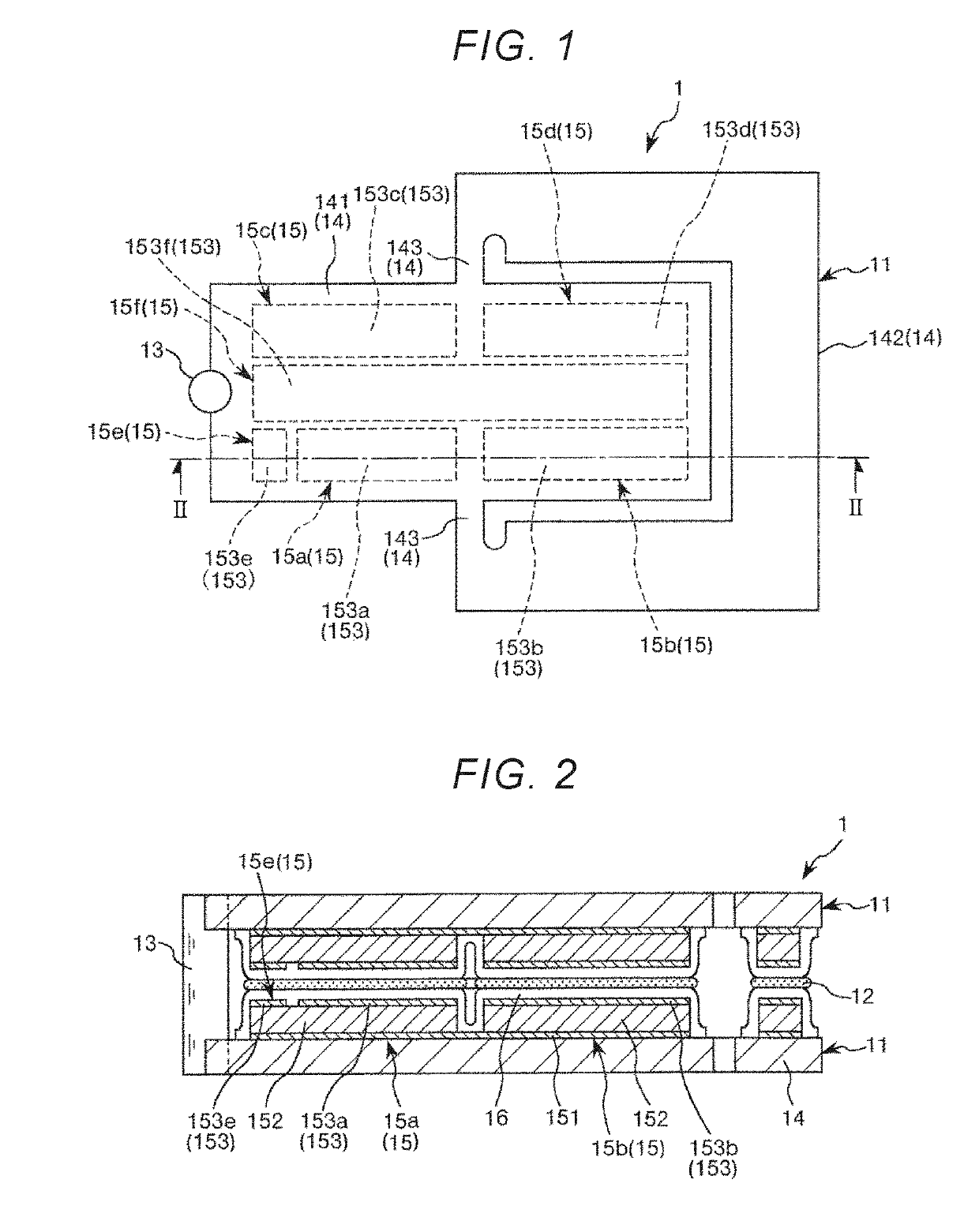
[0060]FIG. 1 is a plan view illustrating the piezoelectric actuator according to a first embodiment of the invention. FIG. 2 is a sectional view taken along line II-II in FIG. 1. Hereinafter, for the sake of convenient description, an upper side in FIG. 2 is referred to as “upper” and a lower side in FIG. 2 is referred to as “lower”.
[0061]As illustrated in FIG. 2, a piezoelectric actuator 1 illustrated in FIG. 1 includes two piezoelectric element units 11, an adhesive layer 12 bonding the two piezoelectric element units 11 to each other, and a projection member 13 bridging the two piezoelectric element units 11. Here, the two piezoelectric element units 11 are configured symmetrically (vertically symmetrical in FIG. 2) with respect to the adhesive layer 12, and have the same configuration as each other.
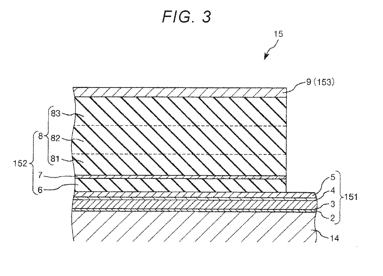
[0062]Each piezoelectric element unit 11 includes a substrate 14, a plurality of piezoelectric elements 15 provided on the substrate 14, and a protective layer 16 covering the plurali...
example 1
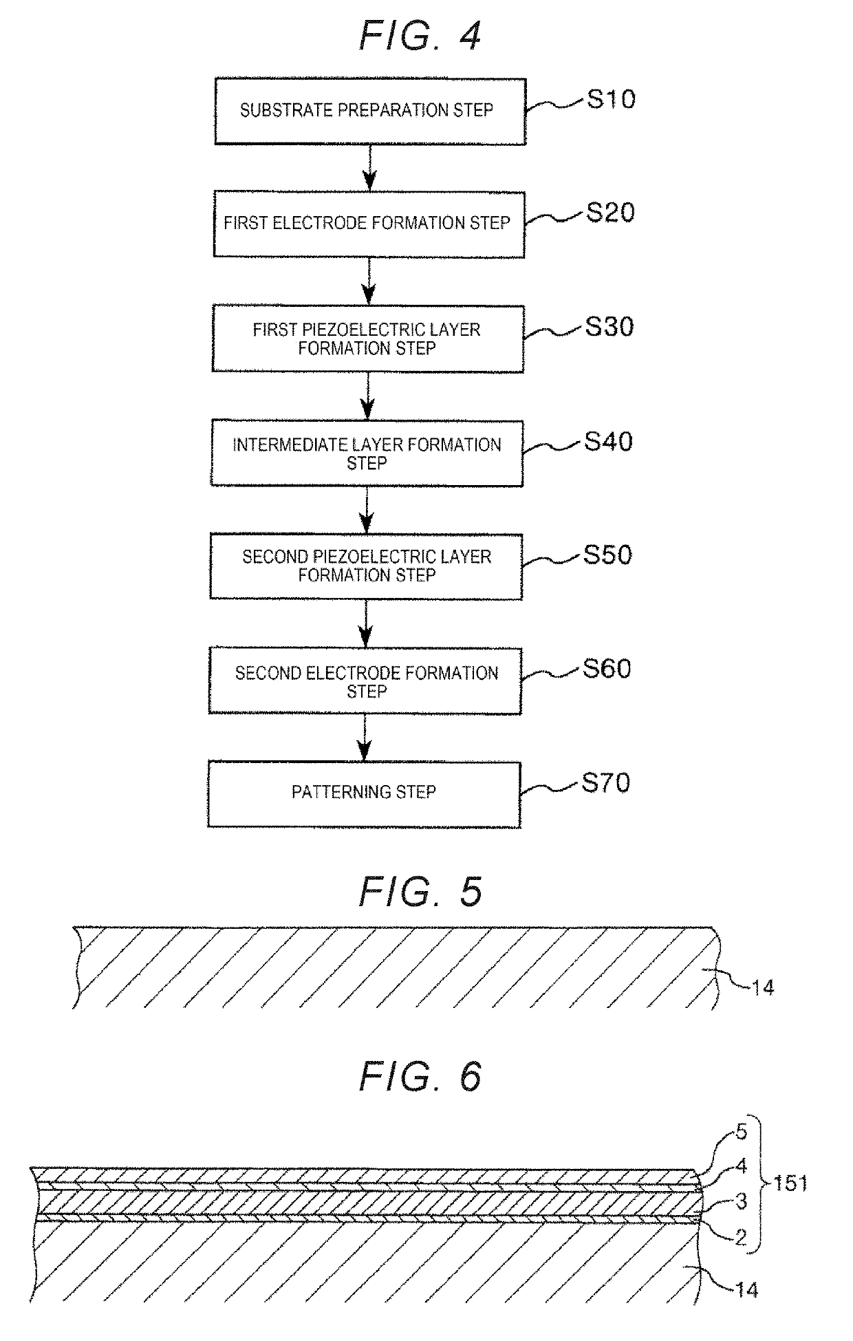
[0148]The piezoelectric actuator illustrated in FIGS. 1 and 2 are manufactured as follows.
[0149]First, a silicon substrate is prepared, and a silicon oxide film with a thickness of 1 μm is formed on one surface of the silicon substrate using thermal oxidation.
[0150]Next, a titanium layer with a thickness of 20 nm, a platinum layer with a thickness of 130 nm, an iridium layer with a thickness of 5 nm, and a titanium layer with a thickness of 4 nm are sequentially formed on a thermal oxide film of the silicon substrate by using a sputtering method, and a first electrode is formed.
[0151]Next, an upper portion of the first electrode is coated with a sol composition of PZT by using an ink jet method, a precursor layer of the PZT is formed by drying the composition, the precursor layer is baked at 740° C. by using rapid thermal anneal (RTA) to crystallize, and thereby, a first piezoelectric layer having a thickness of 110 nm is formed.
[0152]Next, titanium is deposited on the first piezoel...
PUM
Abstract
A piezoelectric actuator includes a vibration portion, a support portion that is integrally configured with the vibration portion and supports the vibration portion, and a piezoelectric element that is disposed on the vibration portion. The piezoelectric element includes a piezoelectric film including columnar crystal grains extending in a thickness direction. When a thickness of the piezoelectric film is referred to as T [μm] and an average diameter of the crystal grains in the width direction is referred to as D [μm], T / D is within a range of 10 to 100. The thickness T of the piezoelectric film is larger than or equal to 2 μm. A standard deviation of diameters of the crystal grains in the width direction is less than or equal to 1.8 μm.
Description
BACKGROUND1. Technical Field[0001]The present invention relates to a piezoelectric actuator, a piezoelectric drive device, a robot, an electronic component transport apparatus, and a printer.2. Related Art[0002]Generally, a piezoelectric element included in a piezoelectric actuator has a structure in which a piezoelectric body is interposed between two electrodes. A piezoelectric element including a piezoelectric body formed by using a sol-gel method is known as the piezoelectric element (refer to, for example, Japanese Patent No. 3903474).[0003]For example, a piezoelectric thin film element according to Japanese Patent No. 3903474 is configured to include a silicon substrate, a siliconoxide film formed on the silicon substrate, a titaniumoxide film formed on the silicon oxide film, a lower electrode formed on the titaniumoxide film, a PZT film formed on the lower electrode, and an upper electrode formed on the PZT film. Here, the PZT film is configured by a polycrystalline body,...
Claims
Application Information
Patent Timeline
Application Date:The date an application was filed.
Publication Date:The date a patent or application was officially published.
First Publication Date:The earliest publication date of a patent with the same application number.
Issue Date:Publication date of the patent grant document.
PCT Entry Date:The Entry date of PCT National Phase.
Estimated Expiry Date:The statutory expiry date of a patent right according to the Patent Law, and it is the longest term of protection that the patent right can achieve without the termination of the patent right due to other reasons(Term extension factor has been taken into account ).
Invalid Date:Actual expiry date is based on effective date or publication date of legal transaction data of invalid patent.

