
Closed chamber for wafer wet processing

a closed chamber and wafer technology, applied in the direction of basic electric elements, semiconductor/solid-state device manufacturing, electric apparatus, etc., can solve the problems of unwanted corrosion of copper on the front side of the wafer, the problem of processing those wafers in an oxygen-containing atmosphere, and the increase of the oxygen content of the air

Active Publication Date: 2012-05-03
LAM RES AG
View PDF7 Cites 305 Cited by
  • Summary
  • Abstract
  • Description
  • Claims
  • Application Information

AI Technical Summary

Benefits of technology

[0009]The present inventor has developed an improved closed chamber module, preferably designed for single wafer wet processing. In the closed chamber module, arms for dispensing media onto a wafer are mounted within t

Problems solved by technology

With increasing miniaturization of the devices fabricated on semiconductor wafers, processing those wafers in an oxygen-containing atmosphere becomes more problematic.
For example, when wafers undergo wet processing in stations that are open to the surrounding air, the oxygen content of the air causes unwanted corrosion of copper on the front side of the wafer.

Method used


Image

  • Closed chamber for wafer wet processing
  • Closed chamber for wafer wet processing
  • Closed chamber for wafer wet processing

Examples


Embodiment Construction

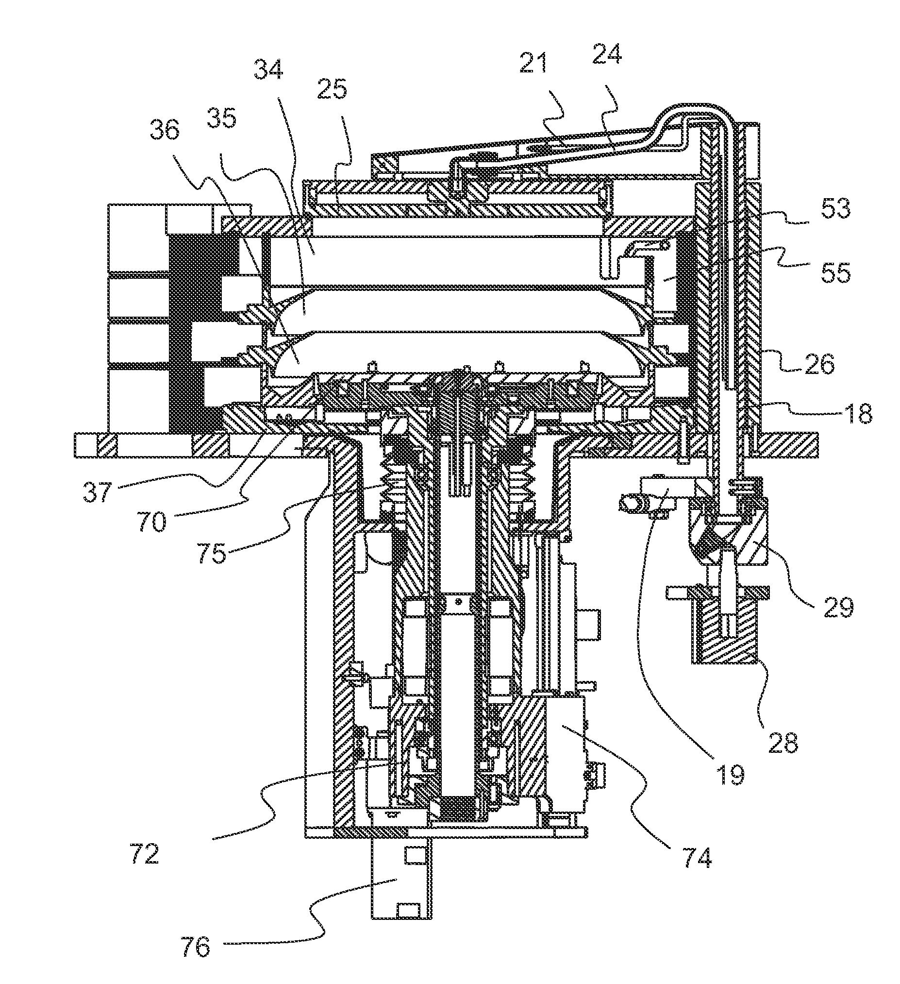
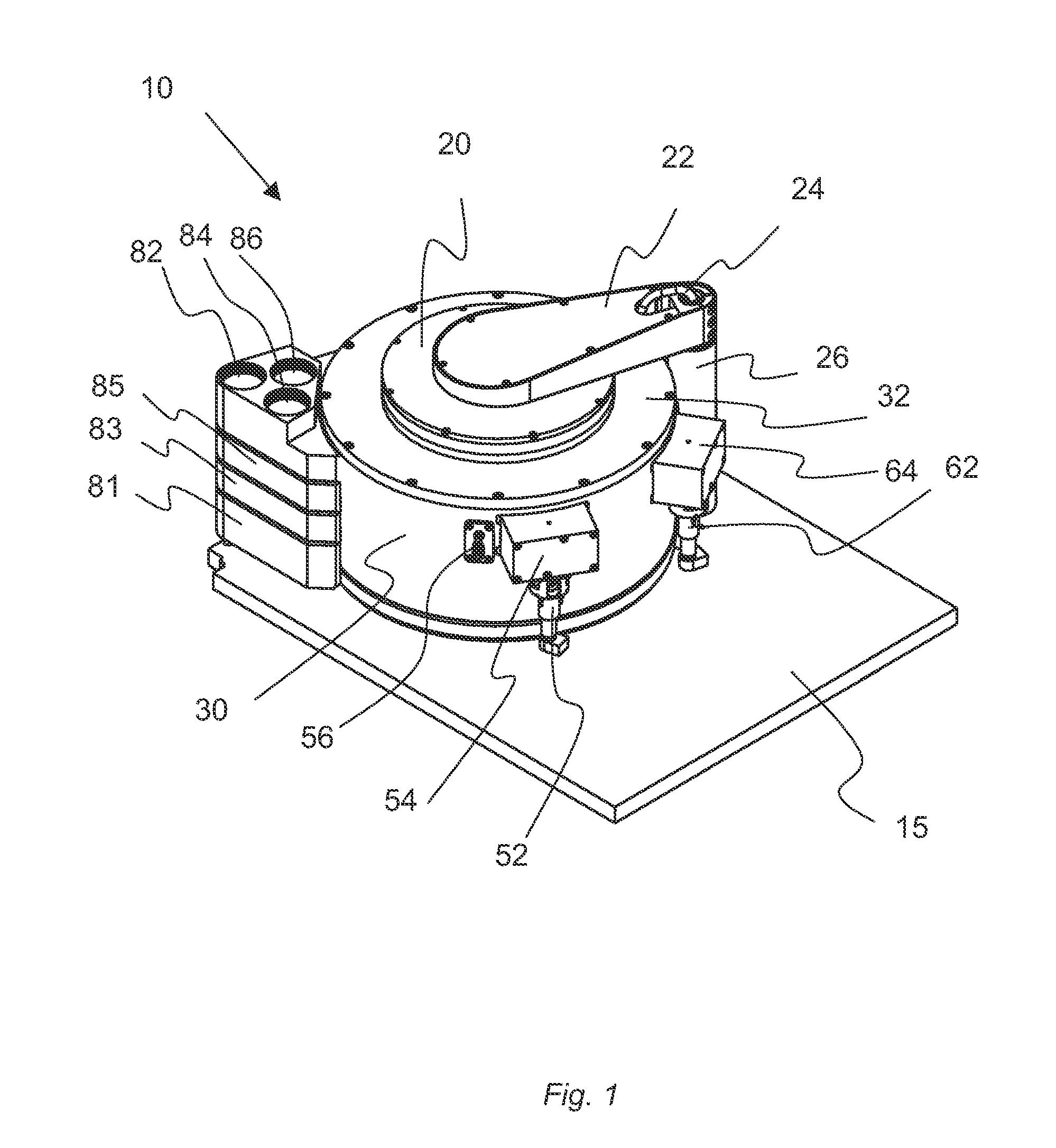
[0022]Referring to FIG. 1, a closed chamber module 10 is mounted on a base plate 15, and is constituted by a preferably cylindrical chamber wall 30 and an annular upper chamber cover 32 secured to the chamber wall 30 by a series of screws or the like. The chamber module 10 is closed at its upper end by shower head lid 10, which seals at its outer periphery to the inner periphery of the annular upper chamber cover 30.

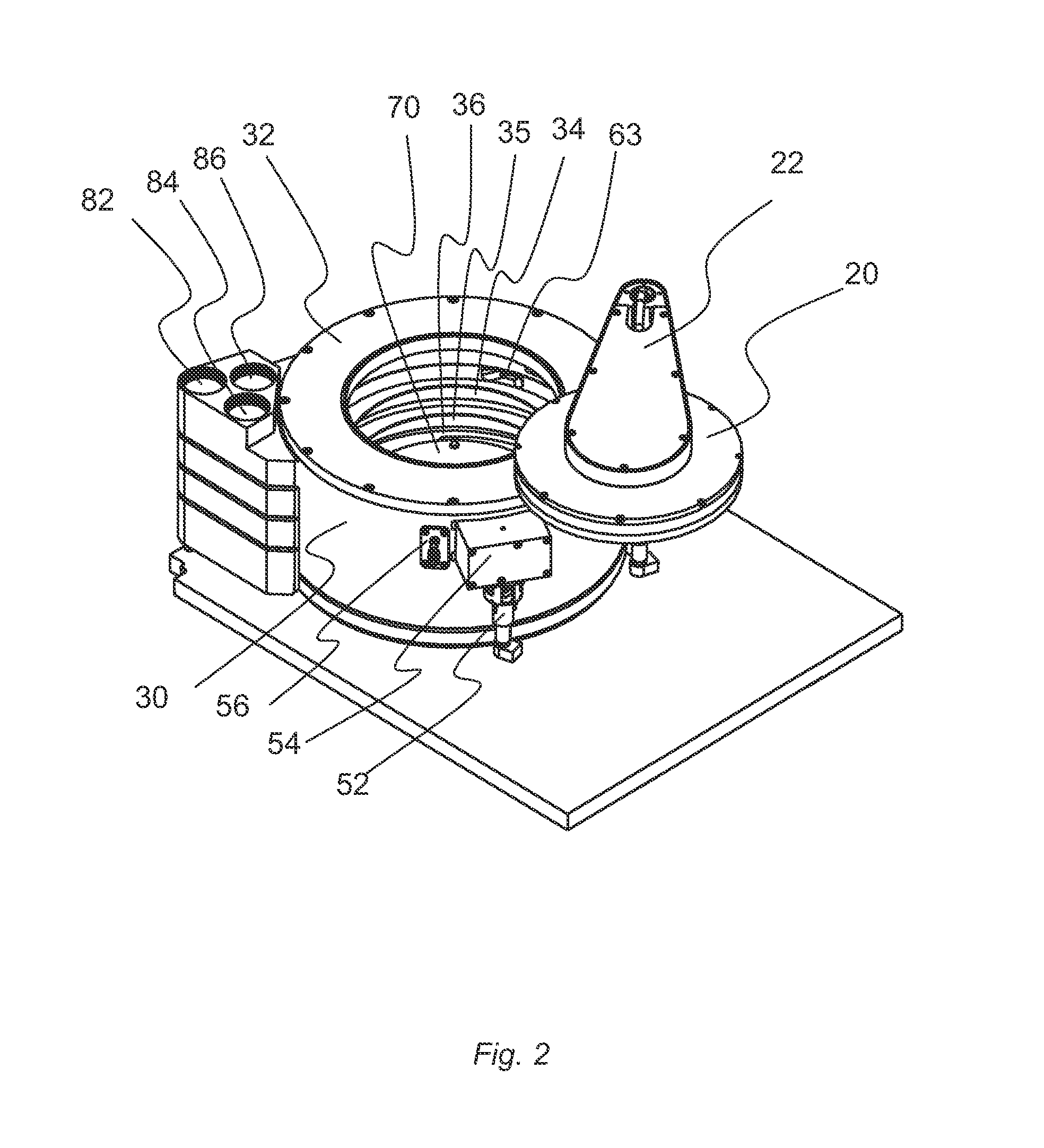
[0023]Lid 20 is secured to lid arm 22, which moves the lid 20 from the closed position shown in FIG. 1 to the open position shown in FIG. 2, and which is in turn positioned on lid support shaft 26. A gas feed line 24 supplies gas to the shower head lid 20.

[0024]First and second drive units 52, 62 are provided for respective media supply arms to be described below, and lead to respective covers 54, 64 for the pivotal movement mechanisms for the media supply arms. Reference numeral 56 denotes a lead-in for the first media supply line.

[0025]The closed chamber module of this...


PUM

PropertyMeasurementUnit
Fractionaaaaaaaaaa
Areaaaaaaaaaaa

Abstract

An improved design for a closed chamber process module for single wafer wet processing utilizes a combination lid and gas showerhead for sealing the chamber from above. One or more media arms dispense liquid onto a wafer in the chamber. The media arms are mounted inside the chamber but are connected by a linkage that passes through the chamber wall to a drive unit mounted outside the chamber.

Description

BACKGROUND OF THE INVENTION[0001]1. Field of the Invention[0002]The invention relates generally to an apparatus for treating surfaces of wafer-shaped articles, such as semiconductor wafers.[0003]2. Description of Related Art[0004]Semiconductor wafers are subjected to various surface treatment processes such as etching, cleaning, polishing and material deposition. To accommodate such processes, a single wafer may be supported in relation to one or more treatment fluid nozzles by a chuck associated with a rotatable carrier, as is described for example in U.S. Pat. Nos. 4,903,717 and 5,513,668.[0005]With increasing miniaturization of the devices fabricated on semiconductor wafers, processing those wafers in an oxygen-containing atmosphere becomes more problematic. For example, when wafers undergo wet processing in stations that are open to the surrounding air, the oxygen content of the air causes unwanted corrosion of copper on the front side of the wafer.[0006]A need therefore exists ...

Claims


Application Information

Patent Timeline
IPC IPC(8): H01L21/465
CPCH01L21/6719H01L21/67126B08B3/00H01L21/304
Inventor HOHENWARTER, KARL-HEINZ
Owner LAM RES AG
Learn More