Supercharge Your Innovation With Domain-Expert AI Agents!

Input/output circuit and method of semiconductor apparatus and system with the same

Active Publication Date: 2012-05-03
SK HYNIX INC
View PDF5 Cites 3 Cited by
  • Summary
  • Abstract
  • Description
  • Claims
  • Application Information

AI Technical Summary

Benefits of technology

[0013]In one exemplary aspect of the present invention, a system includes: a controller which is capable of operating at one of a first speed and a second speed slower than the first speed; a semiconductor memory apparatus operating at the first speed; and an input/output device which is connected between the semiconductor memory apparatus and the controller, and configured to control input/output of signals between

Problems solved by technology

Thus, it is often conceivable that the higher speed semiconductor apparatus cannot be tested for high speed operations in the contemporary test equipment.
However, the investment in the new high speed test equipment requires huge costs, which in turn influences the manufacturing cost and the productivity of a semiconductor apparatus.
In a semiconductor memory apparatus such as a DRAM, the following problems exist in loading a high speed semiconductor memory apparatus on a low speed test equipment and testing the high speed operations of the high speed semiconductor memory apparatus.
First, the low speed test equipment cannot provide the high speed semiconductor memory apparatus with a high speed external clock necessary to ensure high speed operations.
Second, the low speed test equipment is incapable of providing data at a high speed to the high speed semiconductor is memory apparatus.
That is to say, not only the speed of the external clock which is provided to the high speed semiconductor memory apparatus by the low speed test equipment is low, but also the speed at which the low speed test equipment inputs data to the high speed semiconductor memory apparatus is low.
Third, the low speed test equipment is incapable of normally receiving the data which is outputted at a high speed by the high speed semiconductor memory apparatus.
Fourth, the low speed test equipment is incapable of normally receiving the data strobe signal which is outputted at a high speed by the high speed semiconductor memory apparatus.

Method used


Image

  • Input/output circuit and method of semiconductor apparatus and system with the same
  • Input/output circuit and method of semiconductor apparatus and system with the same
  • Input/output circuit and method of semiconductor apparatus and system with the same

Examples


Embodiment Construction

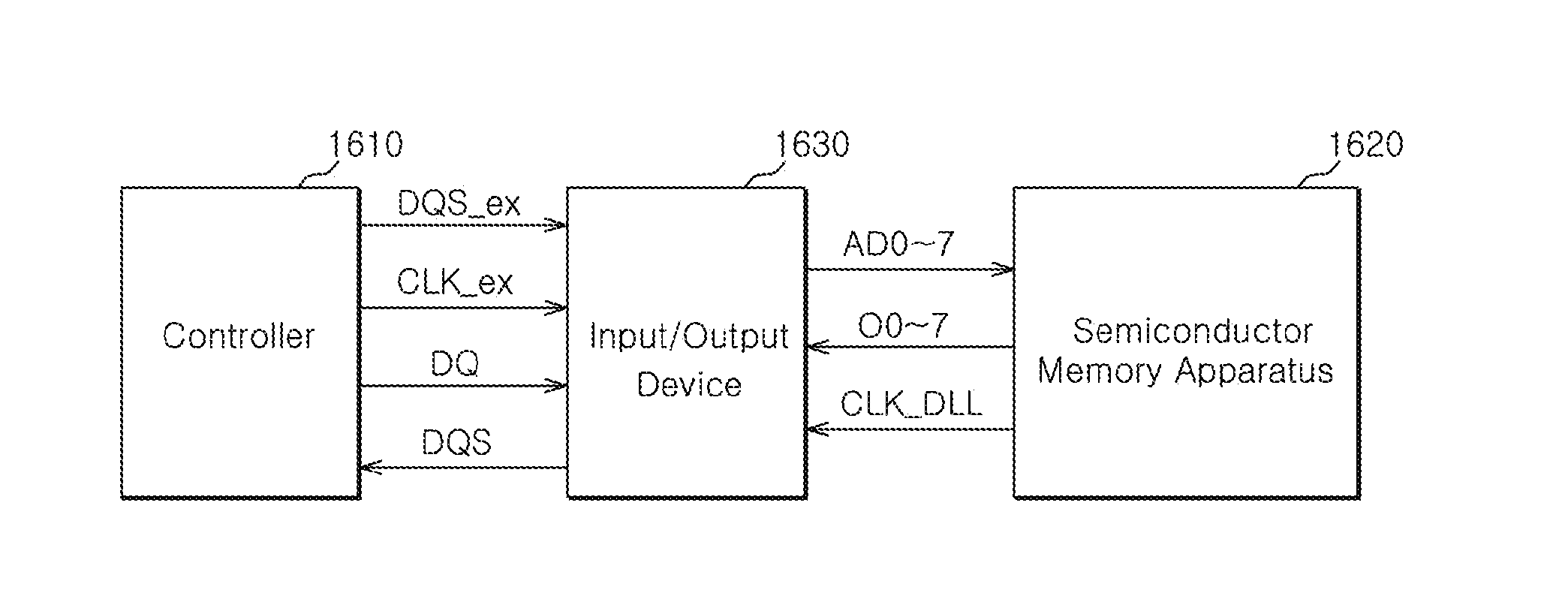
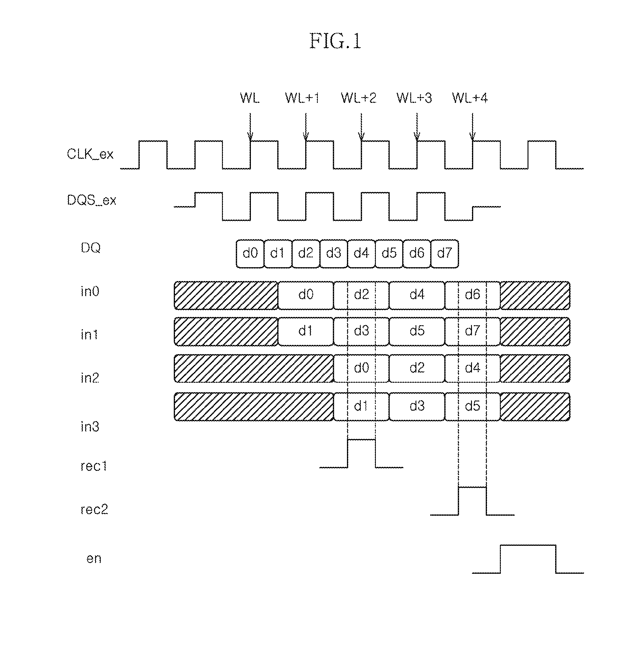
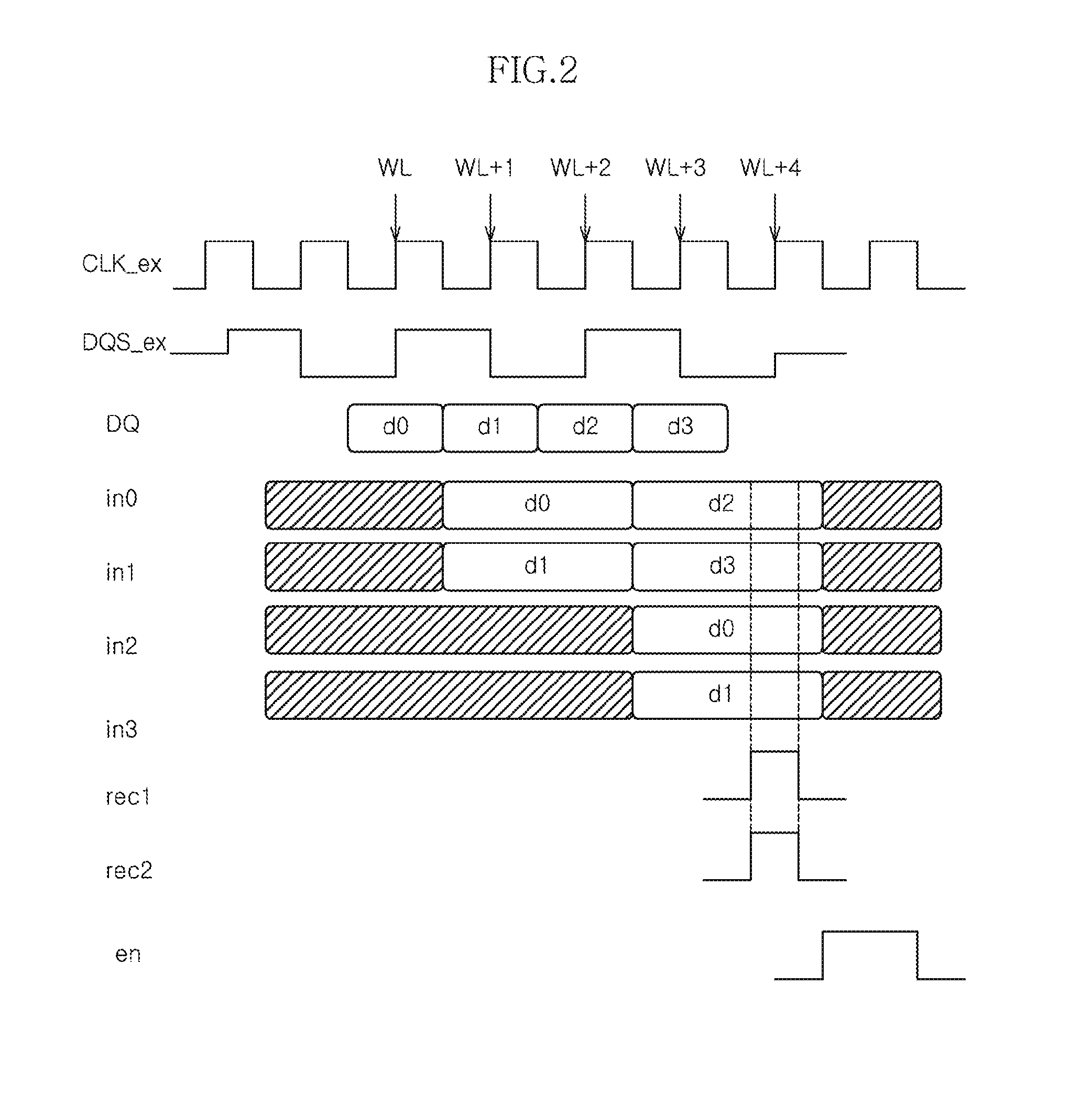
[0036]Hereinafter, an input / output circuit and method of a semiconductor apparatus and a system with the same according to the present invention will be described below with reference to the accompanying drawings through exemplary embodiments.

[0037]Input / output circuits and methods of a semiconductor apparatus in accordance with an embodiment of the present invention solve the above-described problems, which are caused when a low speed test equipment loads a high speed semiconductor apparatus and performs tests for high speed operations, as stated below, so that the low speed test equipment can load the high speed semiconductor apparatus and perform the tests for high speed operations.

[0038]The input / output circuits and methods of the semiconductor apparatus in accordance with the embodiment of the present invention cause at least a portion of input / output signals to be inputted and outputted at a low speed between a test equipment and the semiconductor apparatus so that signals to ...


PUM


Abstract

A system includes a controller which is capable of operating at one of a first speed and a second speed slower than the first speed; a semiconductor memory apparatus operating at the first speed; and an input / output device which is connected between the semiconductor memory apparatus and the controller, and configured to control input / output of signals between the controller and the semiconductor memory apparatus, wherein the input / output device operates in a normal mode which corresponds to the input / output of the signals between the controller operating at the first speed and the semiconductor memory apparatus and a test mode which corresponds to the input / output of the signals between the controller operating at the second speed and the semiconductor memory apparatus.

Description

CROSS-REFERENCES TO RELATED APPLICATION[0001]The present application claims priority under 35 U.S.C. §119(a) to Korean Application No. 10-2010-0106862, filed on Oct. 29, 2010, in the Korean Intellectual Property Office, which is incorporated herein by reference in its entirety as if set forth in full.BACKGROUND[0002]1. Technical Field[0003]Various embodiments of the present invention relates to a semiconductor apparatus, and more particularly, to a semiconductor apparatus including an input / output circuit.[0004]2. Related Art[0005]A semiconductor apparatus is loaded on a test equipment and various tests are performed to check the normal operation and the operation characteristics of a product.[0006]The operation speed and calculation capability of an electronic system are gradually augmented. Accordingly, demand for a higher speed semiconductor apparatus has been increased. As a semiconductor apparatus gradually operates at a higher speed, the operation speed of a semiconductor appa...

Claims


Application Information

Patent Timeline
IPC IPC(8): G11C7/10G11C7/22
CPCG11C29/022G11C29/14G11C29/04G11C2029/5602G11C7/22G11C29/56012
Inventor KIM, KWANG HYUN
Owner SK HYNIX INC
Features
  • R&D
  • Intellectual Property
  • Life Sciences
  • Materials
  • Tech Scout
  • Unparalleled Data Quality
  • Higher Quality Content
  • 60% Fewer Hallucinations
Learn More