Semiconductor device and method of manufacturing the same

Active Publication Date: 2012-05-10
SK HYNIX INC
View PDF3 Cites 10 Cited by
  • Summary
  • Abstract
  • Description
  • Claims
  • Application Information

AI Technical Summary

Benefits of technology

[0006]According to exemplary embodiments, fine patterns may be selectively disconnected or connected by simultaneously etching a pattern, selected from among a plurality of patterns, and patterns neighboring the selected pattern and coupling the neighboring patterns, disconnected by the etch

Problems solved by technology

There are, however, it is difficult to selectively etch only one pattern because an inte

Method used


Image

  • Semiconductor device and method of manufacturing the same
  • Semiconductor device and method of manufacturing the same
  • Semiconductor device and method of manufacturing the same

Examples


Example

[0015]Hereinafter, some exemplary embodiments of the present disclosure will be described in detail with reference to the accompanying drawings. The figures are provided to enable those of ordinary skill in the art to make and use the embodiments of the disclosure.

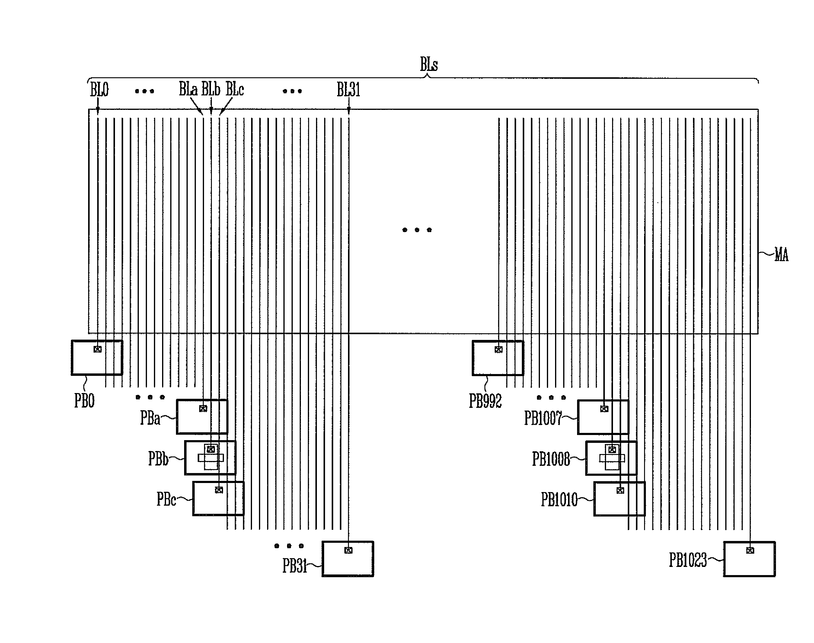
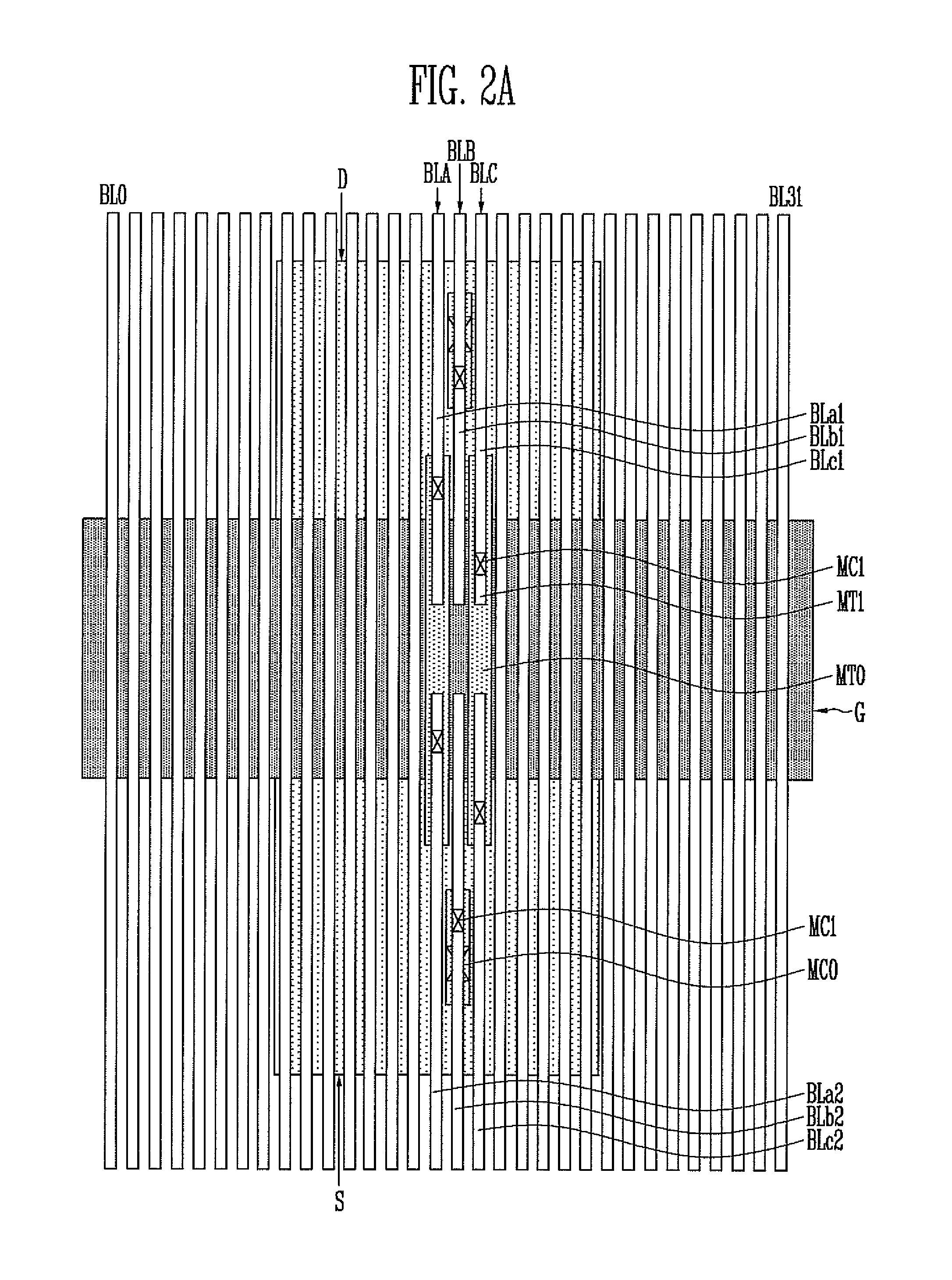
[0016]FIG. 1 is a block diagram illustrating a semiconductor device according to an exemplary embodiment of this disclosure.

[0017]Referring to FIG. 1, in a process of fabricating a semiconductor device, a plurality of line patterns may be formed in parallel. The line patterns are mainly used to couple memory cells and peripheral circuits (for example, sense circuits or page buffers) in a memory device. An example that line patterns are used as the bit lines of a NAND flash memory device is described below.

[0018]In a memory array MA, memory cells are arranged in a column direction and a row direction. The memory cells arranged in the row direction are coupled to the same word line (not shown), and the memory cells arranged ...


PUM


Abstract

A semiconductor device includes a first line pattern and a second line pattern formed in parallel on a semiconductor substrate, third line patterns formed in parallel between the first line pattern and the second line pattern, fourth line patterns formed in parallel between the first line pattern and the second line pattern, a first connection structure configured to couple a first of the third line patterns with a first of the fourth lines patterns, which are adjacent to the first line pattern, and a second connection structure configured to couple a second of the first lines patterns with a second of the fourth lines patterns, which are adjacent to the second line pattern.

Description

CROSS-REFERENCE TO RELATED APPLICATION[0001]Priority to Korean patent application number 10-2010-0110389 filed on Nov. 8, 2010, the entire disclosure of which is incorporated by reference herein, is claimed.BACKGROUND[0002]Exemplary embodiments relate to a semiconductor device and a method of manufacturing the same and, more particularly, to a semiconductor device of fine patterns and a method of manufacturing the same.[0003]In order to increase the degree of integration of semiconductor devices, the width of each of patterns of the semiconductor devices is narrowed, and an interval / space between the patterns (for example, etch mask patterns or conductive patterns) is also be narrowed. A minimum distance between the patterns is determined by the resolution of exposure equipment.[0004]Therefore, a double patterning method for forming patterns having the minimum distance of the exposure equipment therebetween and for additionally forming a pattern between the formed patterns is being ...

Claims


Application Information

Patent Timeline
IPC IPC(8): H01L23/522H01L21/76H01L21/768
CPCH01L23/5226H01L23/528H01L2924/0002H01L2924/00
Inventor SHIN, YONG CHUL
Owner SK HYNIX INC
Why Eureka
Try Eureka