Liquid Crystal Display Device and Manufacturing Method Thereof

Active Publication Date: 2012-05-24
JAPAN DISPLAY INC
View PDF4 Cites 12 Cited by
  • Summary
  • Abstract
  • Description
  • Claims
  • Application Information

AI Technical Summary

Benefits of technology

[0019]In the case of conduction between one of the segments of the pixel electrode and the common electrode, the conducted segment of the pixel electrode is disconnected from the source electrode by applying laser radiation whereby the operation of the other segments of the pixel electrode can be maintained.
[0020]According to the present invention, the pixel in a picture element is divided into the segments. Therefore, even if the common ele

Problems solved by technology

Although a very few pixel defects are allowable, a significant number of pixel defects lead to failure of the liquid crystal disp

Method used


Image

  • Liquid Crystal Display Device and Manufacturing Method Thereof
  • Liquid Crystal Display Device and Manufacturing Method Thereof
  • Liquid Crystal Display Device and Manufacturing Method Thereof

Examples


Example

First Embodiment

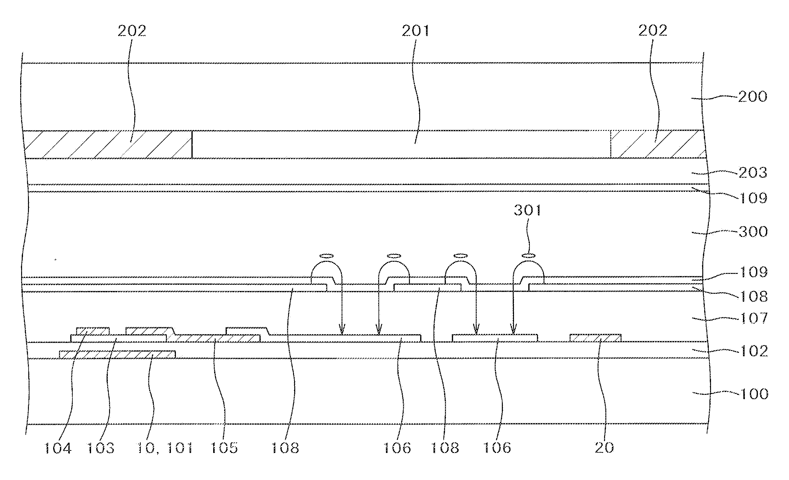
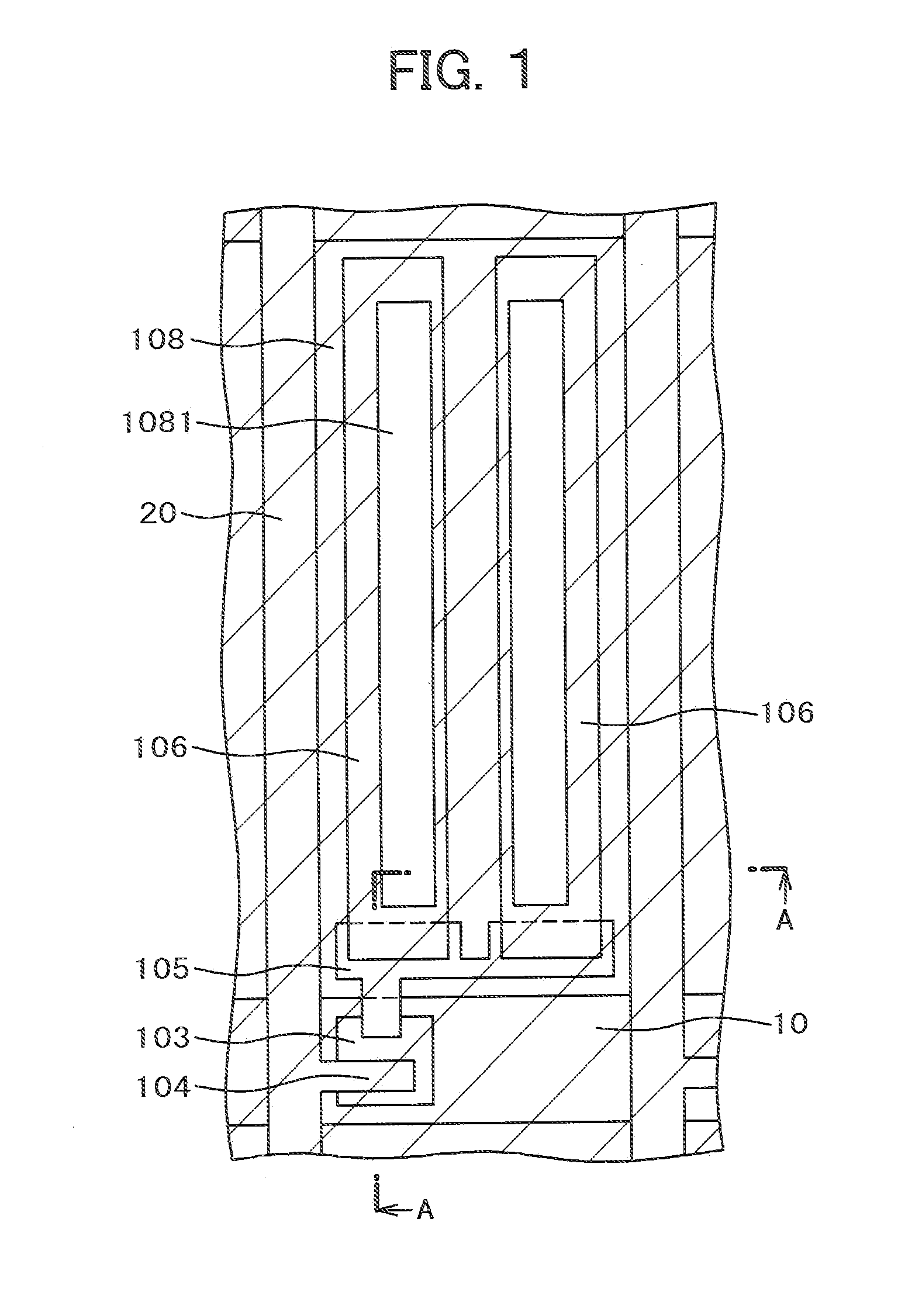
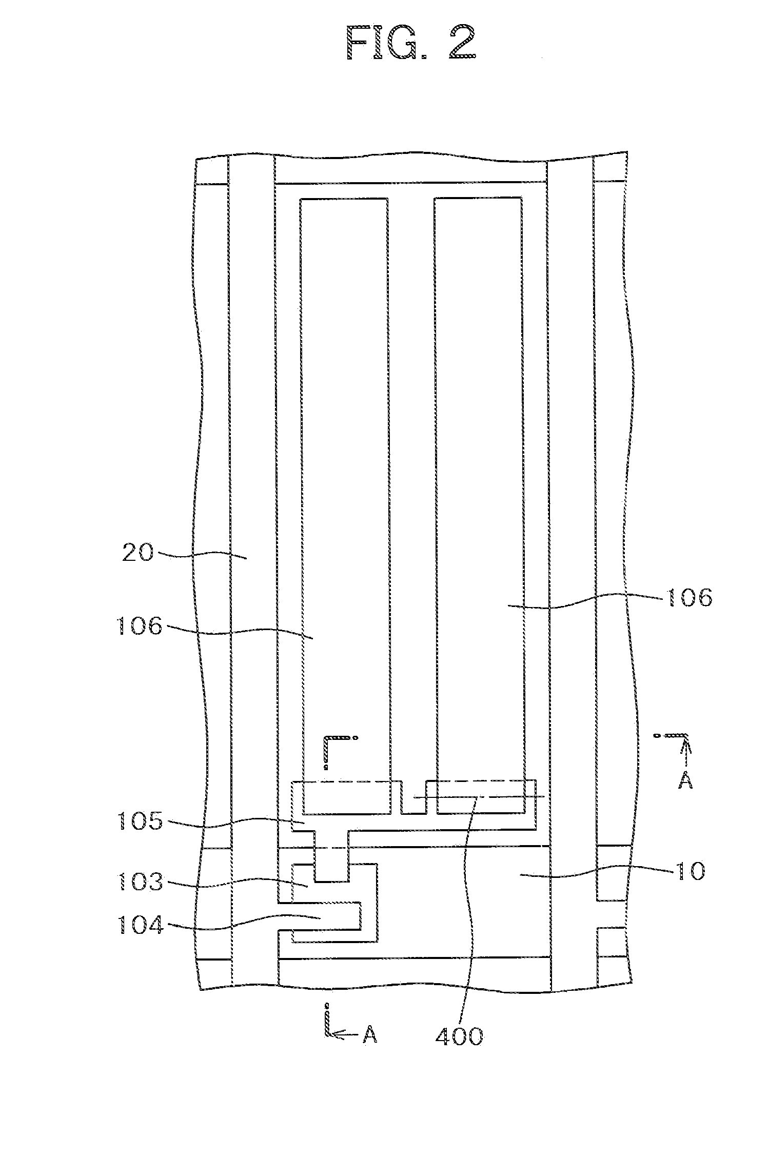
[0039]FIG. 1 is a plan view showing a pixel portion on a TFT substrate 100 according to the present invention. FIG. 2 is a plan view showing the pixel portion of FIG. 1 from which a common electrode 108 is removed. FIG. 3 corresponds to a sectional view taken on the line A-A in FIG. 1, also including a cross-section of a counter substrate 200. Referring to FIG. 1, a pixel electrode 106 is formed on a region enclosed by a picture signal line 20 and a scan line 10. The pixel electrode 106 is divided into two segments. A common electrode 108 formed of a flat solid layer is formed over the pixel electrode 106 with an inter-layer insulating film 107 (not shown) interposed therebetween. In FIG. 1, the common electrode 108 is shown cross-hatched.

[0040]Slits 1081 of the common electrode 108 are located above the pixel electrode 106. Lines of electric force are emitted from the common electrode 108 to the pixel electrode 106 via the slits 1081 in the common electrode 108, so ...

Example

Second Embodiment

[0055]FIG. 9 is a plan view showing a configuration of a pixel portion according to the present invention. The configuration of FIG. 9 is the same as that of FIG. 1 except for the connection between the source electrode 105 and the pixel electrode 106. The difference between FIG. 1 and FIG. 9 is that the segments of the pixel electrode 106 shown in FIG. 1 are overlapped on the source electrode 105 at the connection therewith whereas the source electrode 105 shown in FIG. 9 is overlapped on the segments of the pixel electrode 106. However, the configurations of FIG. 9 and FIG. 1 mean the same in that the source electrode 105 and the segments of the pixel electrode 106 are in direct contact with each other. The configuration of FIG. 9 is characterized by eliminating a problem that development of ITO for forming the pixel electrode 106 does not entail corrosion of the picture signal line 20, the source electrode 105 and the like by a developing solution.

[0056]FIG. 10 i...

Example

Third Embodiment

[0058]FIG. 12 is a plan view showing a pixel configuration according to a third embodiment of the present invention. In FIG. 12, the pixel is centrally formed with the scan line 10 extended in a transverse direction thereof. The lateral sides of the pixel are defined by the picture signal lines 20. Referring to FIG. 12, the pixel consists of a first sub-pixel on the upper side and a second sub-pixel on the lower side. The first sub-pixel is formed with a first pixel electrode 106 while the second sub-pixel is formed with a second pixel electrode 106. The common electrode 108 is laid over the first pixel electrode 106 and the second pixel electrode 106 with the inter-layer insulating film 107 (not shown) interposed therebetween. The common electrode 108 is formed with the slits 1081 at places corresponding to the first pixel electrode 106 and the second pixel electrode 106. In FIG. 12, the common electrode 108 is shown cross-hatched.

[0059]The TFT is formed on the scan...


PUM


Abstract

The present invention seeks to decrease the number of pixel defects in an IPS liquid crystal display device. A gate electrode is formed on a TFT substrate, while a gate insulating film is overlaid on the gate electrode. A pixel electrode which is divided into segments is formed on the gate insulating film. The segments of the pixel electrode are normally interconnected by a source electrode. An inter-layer insulating film, on which a common electrode including slits is formed, is overlaid on the pixel electrode. In a case where the common electrode and one of the segments of the pixel electrode are conductively interconnected by a conductive foreign substance, the other segments of the pixel electrode are allowed to operate by disconnecting the conducted segment of the pixel electrode from the source electrode. Thus, one pixel is prevented from lapsing into a full pixel defect.

Description

CLAIM OF PRIORITY[0001]The present application claims priority from Japanese Patent Application JP 2010-261153 filed on Nov. 24, 2010, the content of which is hereby incorporated by reference into this application.BACKGROUND OF THE PRESENT INVENTION[0002]1. Field of the Present Invention[0003]The present invention relates to a display device. More particularly, the present invention relates to a liquid crystal display device of horizontal electric field type which is adapted to increase fabrication yield and to decrease manufacturing cost.[0004]2. Related Arts[0005]A liquid crystal display panel for use in liquid crystal display device includes: a TFT substrate on which pixels, each including a pixel electrode, a thin film transistor (TFT) and the like are arranged in a matrix form; a counter substrate opposed to the TFT substrate and formed with a color filter and the like in corresponding relation to the pixel electrode of the TFT substrate; and liquid crystal sandwiched between t...

Claims


Application Information

Patent Timeline
IPC IPC(8): G02F1/1343G02F1/1368
CPCG02F2001/134372G02F1/134309G02F1/134372
Inventor NAGAMI, TAKAHIRO
Owner JAPAN DISPLAY INC
Why Eureka
Try Eureka