Regrown heterojunction bipolar transistors for multi-function integrated devices and method for fabricating the same

Active Publication Date: 2012-05-31
TELEDYNE SCI & IMAGING
View PDF4 Cites 3 Cited by
  • Summary
  • Abstract
  • Description
  • Claims
  • Application Information

AI Technical Summary

Benefits of technology

[0011]In yet another embodiment, the present invention may provide a method for fabricating an integrated device, which may have a first heterojunction bipolar transistor (HBT) device formed on a first region of a substrate and a second HBT device formed on a second region of the substrate, and in which the first region may be spaced apart from the second region. The method may include the steps of depos

Problems solved by technology

However, due to various technical issues, the ion implantation process is generally not used for collector doping of these compound semiconductor HBT devices.
However, multiple substrates may lead to additional parasitic effects and inter-chip routing.
As such, it may become inefficient for multi-function integrated devices to have multiple HBT devices with different collector doping profiles.

Method used


Image

  • Regrown heterojunction bipolar transistors for multi-function integrated devices and method for fabricating the same
  • Regrown heterojunction bipolar transistors for multi-function integrated devices and method for fabricating the same
  • Regrown heterojunction bipolar transistors for multi-function integrated devices and method for fabricating the same

Examples


Embodiment Construction

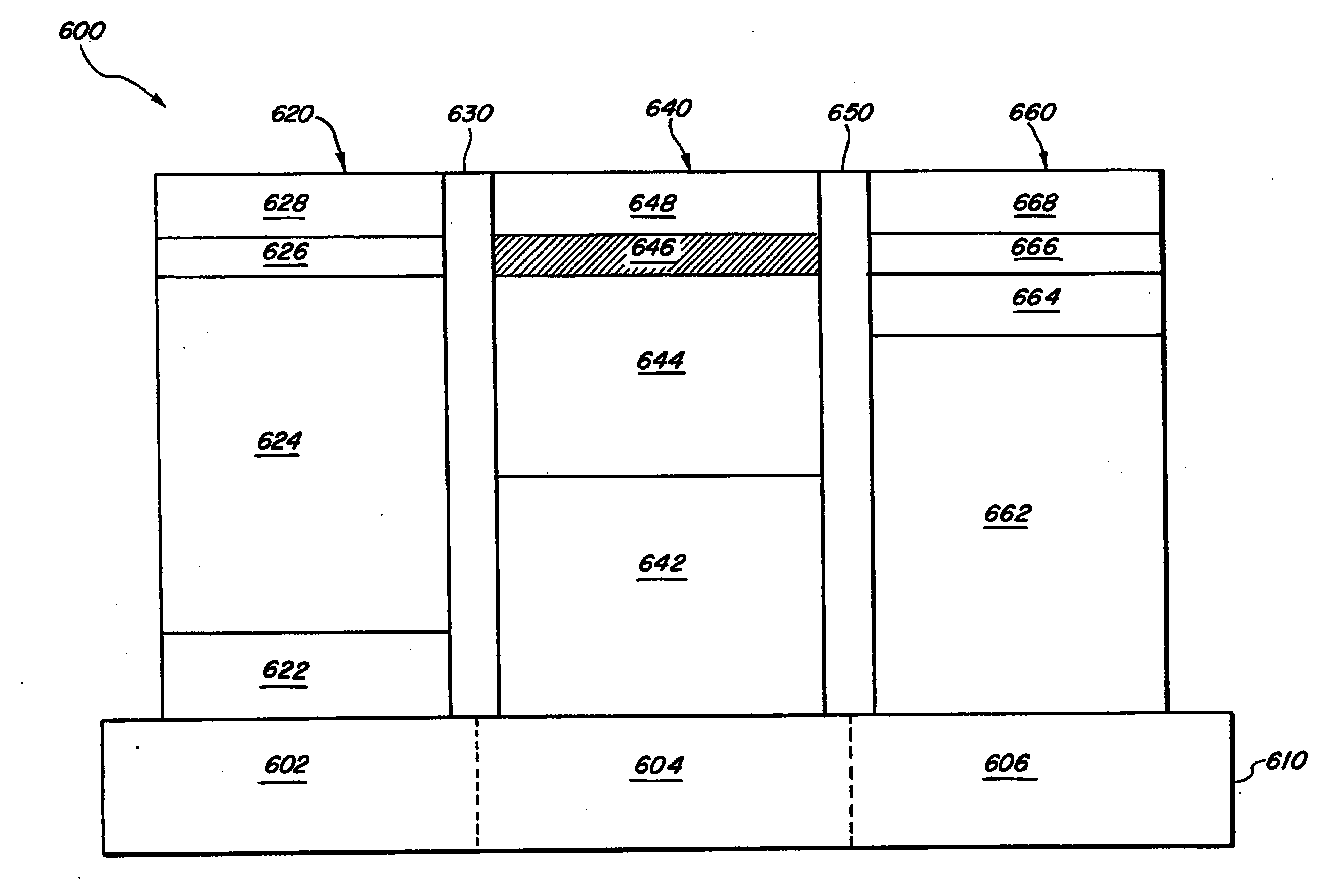
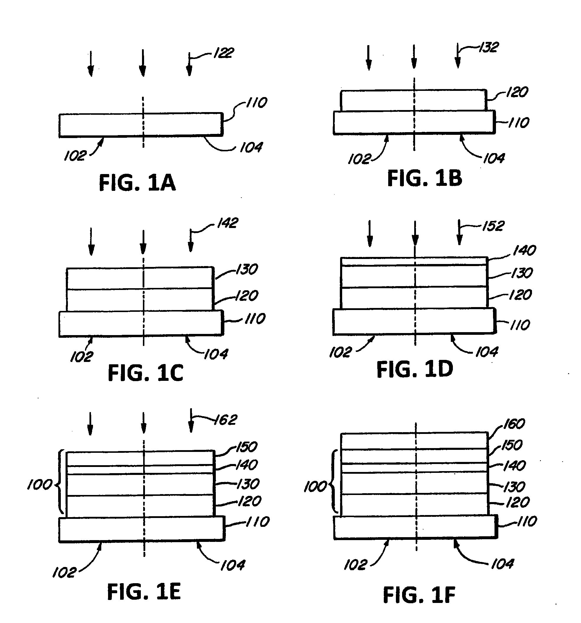
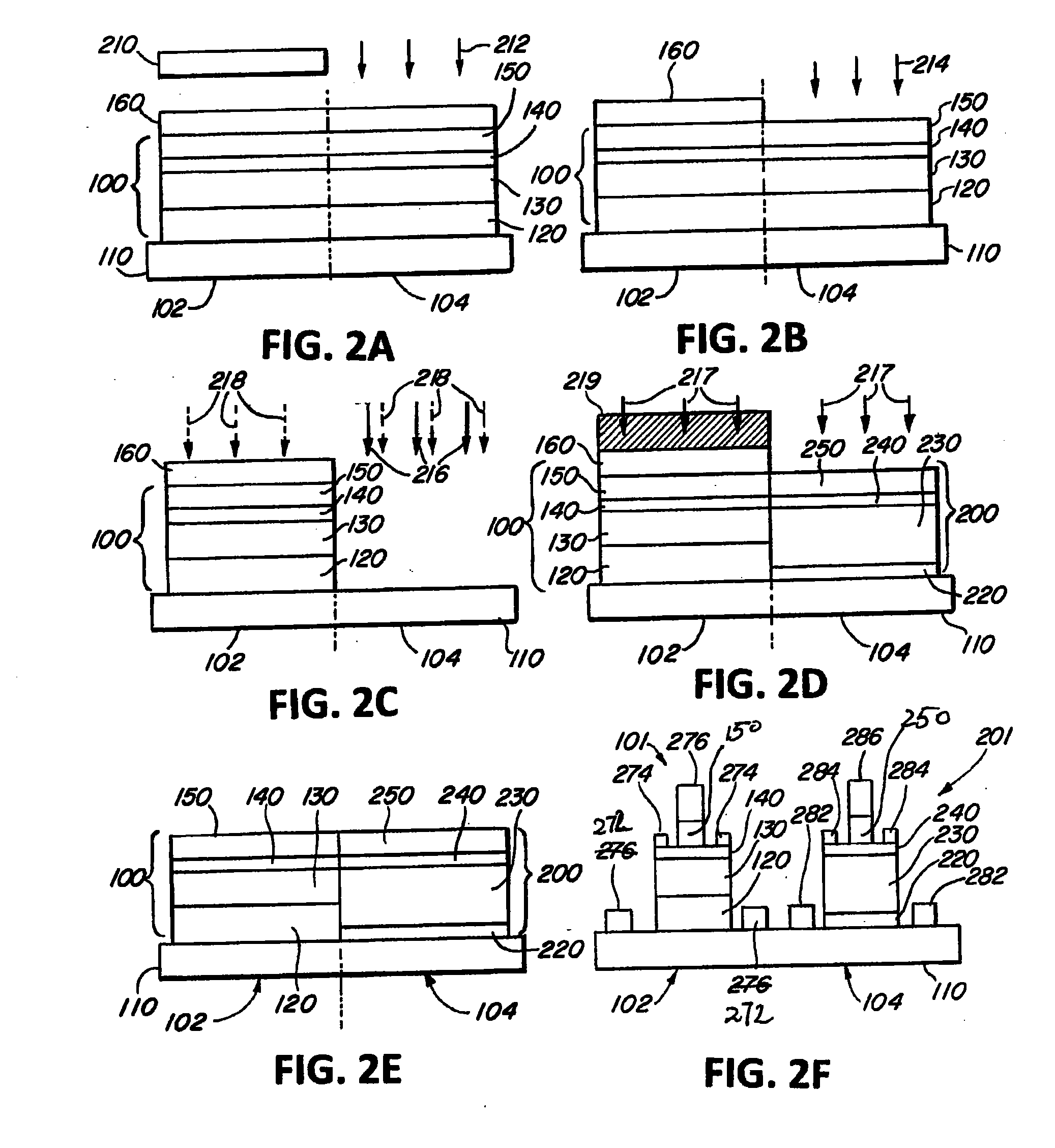
[0023]Apparatus, systems and methods that implement the embodiment of the various features of the present invention will now be described with reference to the drawings. The drawings and the associated descriptions are provided to illustrate some embodiments of the present invention and not to limit the scope of the present invention. Throughout the drawings, reference numbers are re-used to indicate correspondence between reference elements. In addition, the first digit of each reference number indicates the figure in which the element first appears.

[0024]Throughout this disclosure, the term “processing” in the context of forming a wafer layer includes, but is not limited to, coating a layer with insulating or conductive material using a deposition process, patterning a layer using a masking or etching process, preparing the layer for bonding by depositing bond pads such as gold bond pads onto the surface of a layer, and / or removal of material from or complete removal of one or mor...


PUM


Abstract

The present invention may provide an integrated device, which may include a substrate having first and second regions, the first region spaced apart from the second region, a first heterojunction bipolar transistor (HBT) device formed on the first region of the substrate, the first HBT device having a first collector layer formed above the first region of the substrate, the first collector layer having a first collector thickness and a first collector doping level, and a second HBT device formed on the second region of the substrate, the second HBT device having a second collector layer formed above the second region of the substrate, the second collector layer having a second collector thickness and a second collector doping level, the second collector thickness substantially greater than the first collector thickness, the second collector doping level lower than the first collector doping level.

Description

BACKGROUND[0001]1. Field[0002]The present invention relates generally to the field of regrown bipolar transistors, and more particularly to regrown heterojunction bipolar transistors (HBT) for multi-function integrated circuits and method for fabricating the same.[0003]2. Description of the Related Art[0004]Compared to conventional silicon-based homojunction bipolar junction transistors (BJT), a heterojunction bipolar transistor (HBT) may have an emitter layer with a larger bandgap and a base layer with a smaller bandgap. The larger bandgap emitter layer may provide a better barrier for hole injection, which may be initiated from the base layer. Accordingly, the base layer may be doped at a higher doping level, thereby lowering the base resistance and improving the radio frequency (RF) performance of the HBT.[0005]For conventional silicon-based homojunction BJT, the collector doping may be performed by an ion implantation process, which may allow the collector layers of various BJT ...

Claims


Application Information

Patent Timeline
IPC IPC(8): H01L29/737H01L21/8222
CPCH01L21/8252H01L29/7371H01L29/0821H01L27/0605
Inventor URTEAGA, MIGUEL E.
Owner TELEDYNE SCI & IMAGING
Why Eureka
Try Eureka