
Switching device and a method for forming a switching device

a technology of switching device and switching device, which is applied in the direction of relays, static storage, instruments, etc., can solve the problems of large area footprint, difficult mass fabrication of these, and high cost of memory or computing usag

Inactive Publication Date: 2012-06-07
AGENCY FOR SCI TECH & RES
View PDF2 Cites 17 Cited by
  • Summary
  • Abstract
  • Description
  • Claims
  • Application Information

AI Technical Summary

Benefits of technology

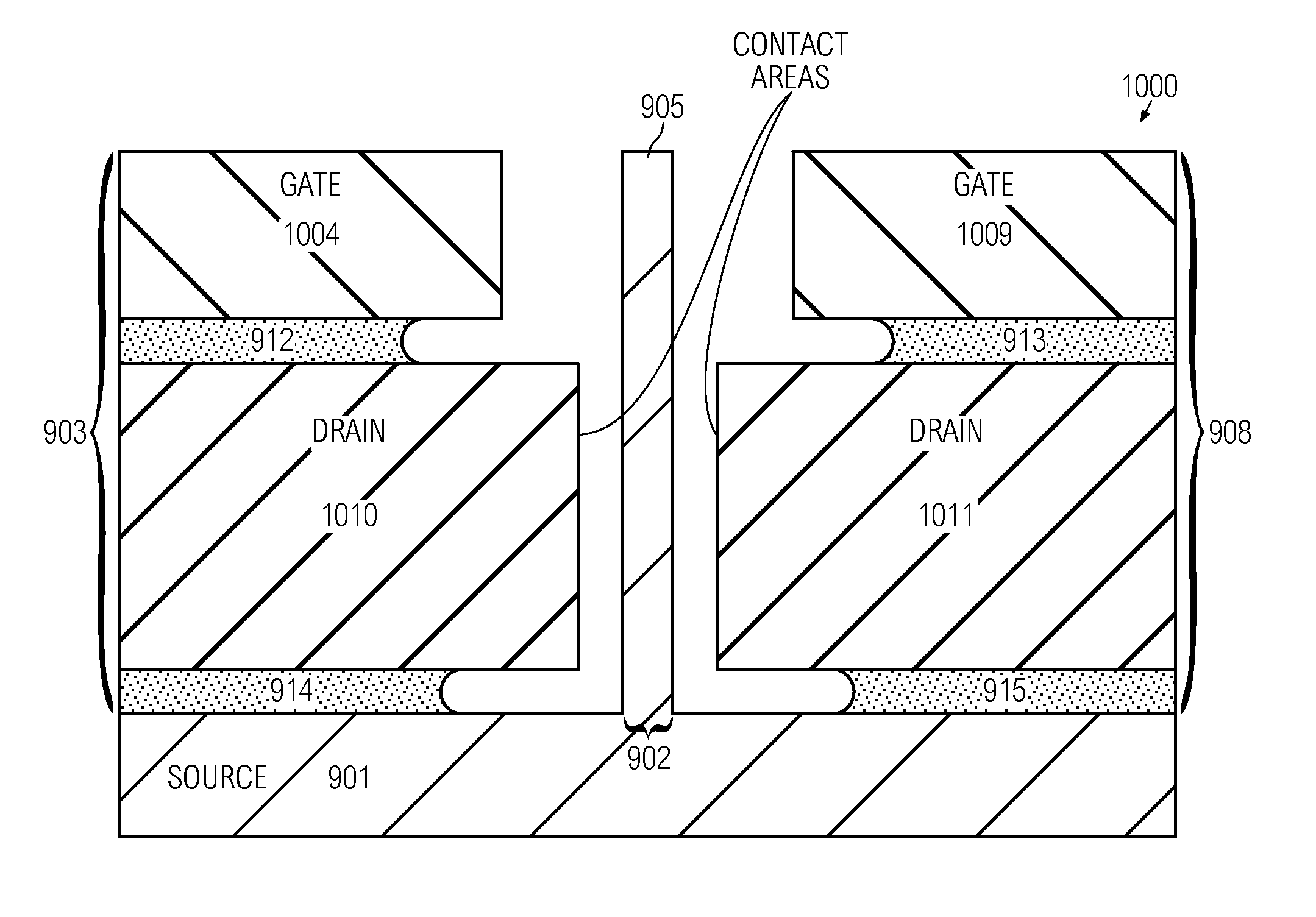
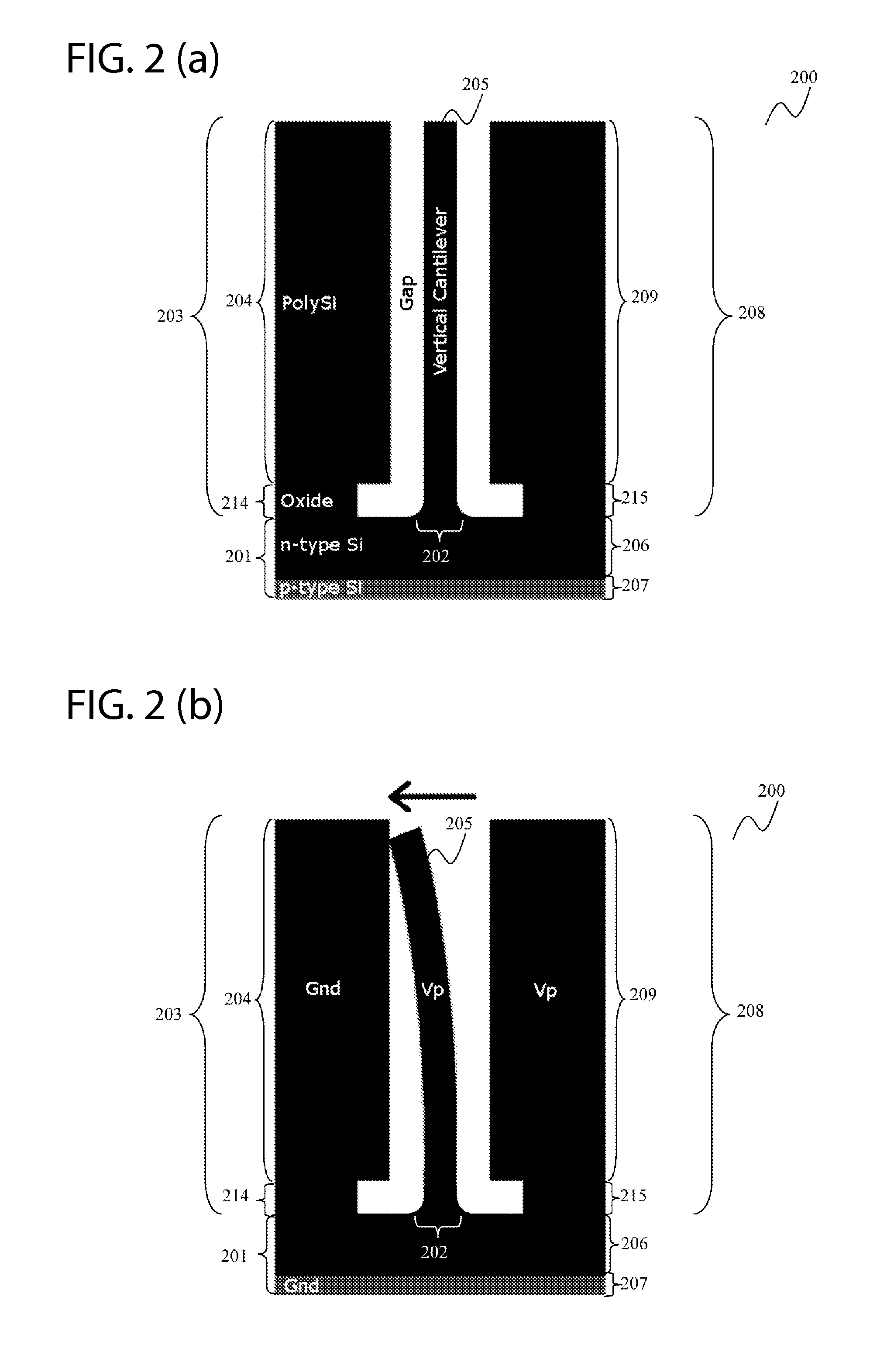
[0006]In one embodiment, a switching device is provided. The switching device may include a substrate. The substrate may include a contact region. The switching device may further include a vertical layer arrangement extending from the substrate next to the contact region, wherein the vertical layer arrangement includes a control layer. The switching device may further include a freestanding silicon cantilever extending vertically from the contact region.

Problems solved by technology

A major challenge of NEM switches has been their density—horizontally oriented cantilever NEM switches with CMOS-compatible processes have been demonstrated for memory use, but these traditionally incur a large area footprint, making them expensive for memory or computing usage.
Vertically oriented switches have been proposed previously based on multiwall carbon nanotubes (MWCNTs), but the mass fabrication of these remains difficult and costly.

Method used


Image

  • Switching device and a method for forming a switching device
  • Switching device and a method for forming a switching device
  • Switching device and a method for forming a switching device

Examples


Embodiment Construction

[0073]The following detailed description refers to the accompanying drawings that show, by way of illustration, specific details and embodiments in which the invention may be practiced. These embodiments are described in sufficient detail to enable those skilled in the art to practice the invention. In this regard, directional terminology, such as “top”, “bottom”, “front”, “back”, “leading”, “trailing”, etc, is used with reference to the orientation of the Figure(s) being described. Because components of embodiments can be positioned in a number of different orientations, the directional terminology is used for purposes of illustration and is in no way limiting. Other embodiments may be utilized and structural, logical, and electrical changes may be made without departing from the scope of the invention. The various embodiments are not necessarily mutually exclusive, as some embodiments can be combined with one or more other embodiments to form new embodiments. The following detaile...


PUM


Abstract

Embodiments provide a switching device. The switching device includes a substrate, which includes a contact region. The switching device further includes a vertical layer arrangement extending from the substrate next to the contact region. The vertical layer arrangement includes a control layer. The switching device further includes a freestanding silicon cantilever extending vertically from the contact region.

Description

[0001]The present application claims the benefit of the Singapore patent application 201008259-2 (filed on 4 Nov. 2010), the entire contents of which are incorporated herein by reference for all purposes.Field of the Inventions[0002]Embodiments relate generally to a switching device and a method for forming a switching device.BACKGROUND OF THE INVENTIONS[0003]Nanoelectromechanical (NEM) switches have been proposed by many for non-volatile memory applications because of their low power consumption and nanosecond range switching speeds, which translate to write or erase speeds several orders of magnitude faster than NAND Flash. NEM switches have been also suggested as an answer to the high leakage current limitation of scaling CMOS transistors further. NEM switches offer zero leakage, high sub-threshold slopes and are an attractive for scaling as well as low power computing. Furthermore, NEM switches are able to withstand harsh environments (high temperatures and radiation dosages), a...

Claims


Application Information

Patent Timeline
Patent Type & Authority Applications(United States)
IPC IPC(8): H01H59/00H01L21/00
CPCG11C13/025G11C2213/16H01H59/0009H01H1/0094
Inventor NG, JIAQIANG ELDWINTSAI, MING LIN JULIUSSINGH, NAVABSHEN, NANSHENG
Owner AGENCY FOR SCI TECH & RES
Learn More