RFID readable device with smart surface access

a technology of readable devices and smart surfaces, applied in the field of radio frequency identification devices (rfid) systems, can solve the problems of laborious near-field coupling of a reader with every tag device of a tablecloth array having a very large number of sensing nodes over a relatively large surface area, and achieve the effect of minimizing power loss

Inactive Publication Date: 2012-06-07
STMICROELECTRONICS SRL
View PDF13 Cites 0 Cited by
  • Summary
  • Abstract
  • Description
  • Claims
  • Application Information

AI Technical Summary

Benefits of technology

[0013]In case simple tag devices are coupled to the sensing nodes, a RFID surface device is implemented, whereby the tag devices are energized by the reader. If the sensing nodes are coupled to active self-powered sensor / actuator devices, then a “surface sensor network” device is implemented. In this case the smart surface RFID network may have a main requirement of minimizing power losses along the data transfer paths between any sensing node and the reader. If the sensing nodes are coupled in part passive tags / passive sensors and in part active sensors and / or actuators, then the smart surface RFID network will serve for exchanging data among the sensing nodes and between the active sensors / actuators and the reader, as well as for powering the passive tags and passive sensors.

Problems solved by technology

However, self-consistency of each individual cell follows the conventional approach of a pixel type organization, and is burdensome specially for sensing events that may occur at any location over a relatively large surface of a structure or body to be monitored.
Communications with the external board by OLED devices and the embedding of a photovoltaic generator, battery or other energy storing device in each individual cell may be burdensome.
Near-field coupling of a reader with every tag device of a tablecloth array having a very large number of sensing nodes over a relatively large surface is labor intensive.

Method used


Image

  • RFID readable device with smart surface access
  • RFID readable device with smart surface access
  • RFID readable device with smart surface access

Examples


Embodiment Construction

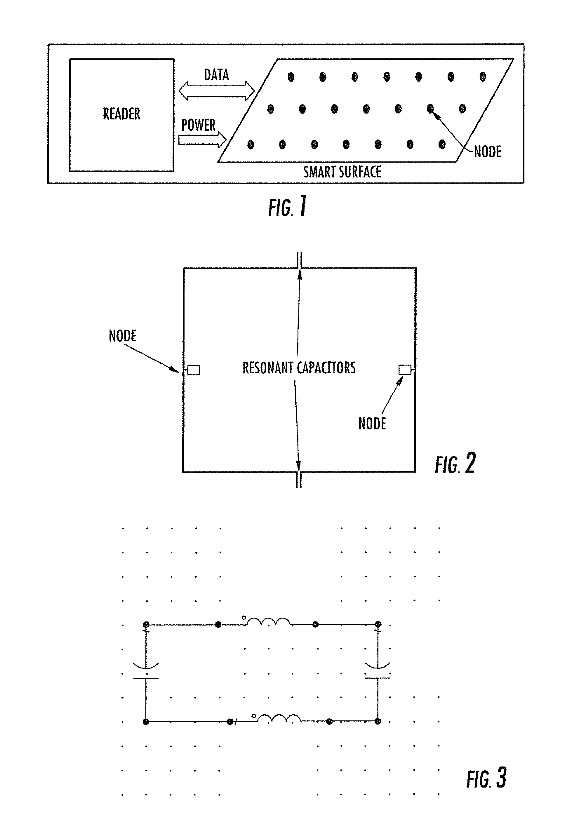
[0022]FIG. 1 is an exemplary scheme of a near-field and / or far-field RF accessible multi-node surface monitoring device. The array has a plurality of sensing nodes that may be uniformly spaced as depicted, or may have any kind of distribution over the surface according to the monitoring needs. The reader device is typically a remote unit that may be fixed or mobile.

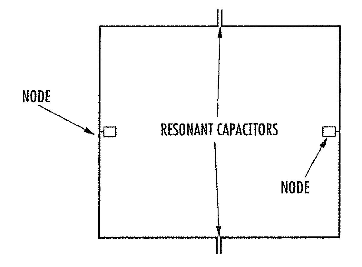
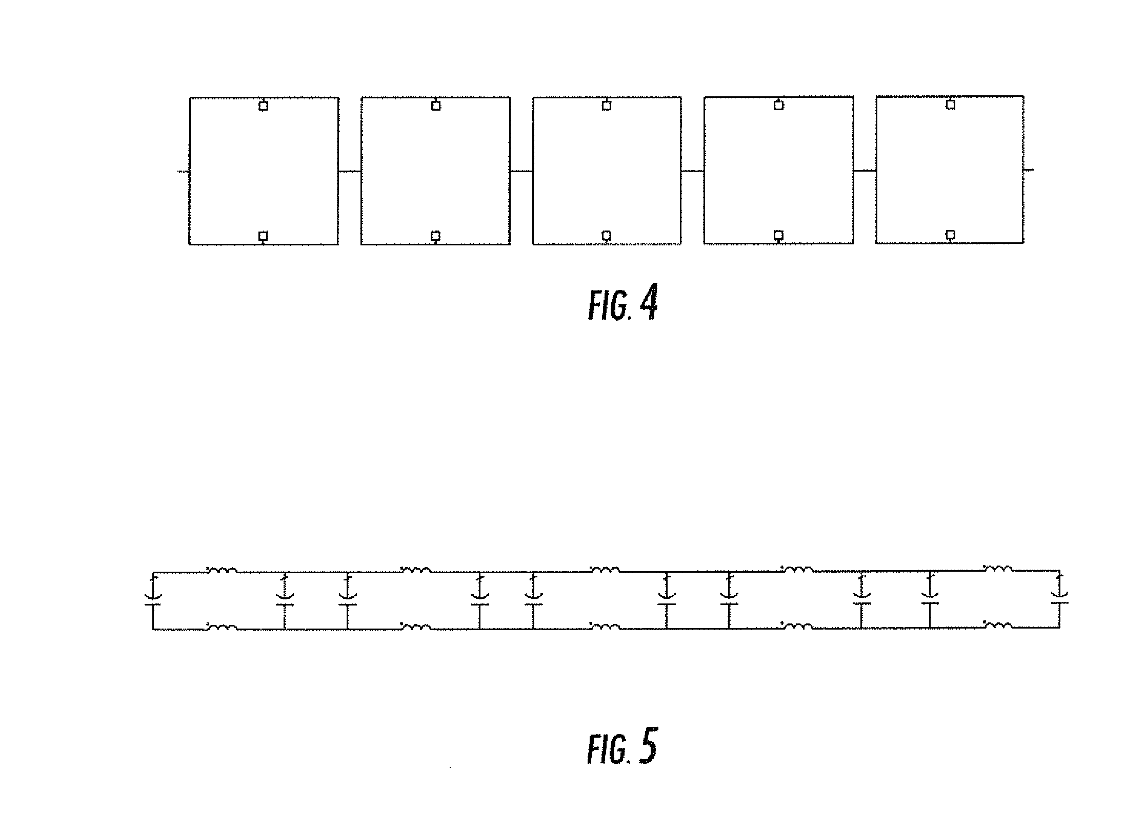
[0023]FIGS. 2 and 3 are a basic layout and the equivalent circuit, respectively, of a RF coupling structure between two adjacent nodes of a multi-node surface monitoring device. The RF coupling structure may, for example, be realized in any of the forms extensively described in great detail in patent application no. US2009 / 0033467, which is assigned to the assignee of the present invention and the entire contents of which are incorporated by reference. Of course, other specifically developed more effective near-field and far-field RF coupling structures may be used to implement a bi-dimensional smart surface coupling netw...


PUM


Abstract

A monitoring system includes an array of concatenated sensing nodes, with each sensing node being configured to have at least one of near-field and far-field RF coupling circuitry to interface with an adjacent sensing node. A respective device is coupled to each of the sensing nodes. A reader device is configured to have at least one of near-field and far-field RF coupling circuitry to interface with the array of concatenated sensing nodes to read data from the devices.

Description

FIELD OF THE INVENTION[0001]The present disclosure relates generally to Radio Frequency Identification Device (RFID) systems, and, in particular, to large surface systems with a mono-dimensional or bi-dimensional array of sensing nodes.BACKGROUND OF THE INVENTION[0002]There are ongoing projects to devise approaches to monitor for prolonged periods of time, and ideally, even permanently, tag data, physical, chemical and / or geometrical parameter changes that may occur at any spot location over large structures.[0003]Patent application no. VA2010A000018, assigned to the current assignee of the present invention and filed on Feb. 26, 2010, describes a multi-cell flexible sheet of organic polymer construction and having a finite or a theoretically unlimited length. The multi-cell flexible sheet includes a monolithically fabricated array of one or more types of cells having the same or different functionalities (e.g., sensor cells, active pixel cells of a large size display). The cells ar...

Claims


Application Information

Patent Timeline
Patent Type & Authority Applications(United States)
IPC IPC(8): G01R27/04
CPCH04B5/0031H04B5/0037H02J5/005H04B5/0062H04B5/0043H02J50/12
Inventor GIRLANDO, GIOVANNI
Owner STMICROELECTRONICS SRL
Why Eureka
Try Eureka