Organic Light-Emitting Display Device and Method of Manufacturing the Same

a technology of light-emitting display and organic materials, which is applied in the direction of semiconductor devices, electrical devices, transistors, etc., can solve the problems of increasing manufacturing costs, increasing manufacturing time, and increasing manufacturing costs, and achieves the effect of improving aperture ratio and simple process

Active Publication Date: 2012-06-14
SAMSUNG DISPLAY CO LTD
View PDF4 Cites 78 Cited by
  • Summary
  • Abstract
  • Description
  • Claims
  • Application Information

AI Technical Summary

Benefits of technology

[0009]The present invention provides an organic light-emitting display device manufactured via a simple process and having an improved aperture ratio, and a method of manufacturing the organic light-emitting display device.

Problems solved by technology

As described above, in the process of transferring the pattern by using the mask, it is necessary to first arrange a mask having a desired pattern, and thus manufacturing costs for preparing masks increase as the number of processes using the masks increases.
Also, in the process, the aforementioned complicated operations have to be performed, which results in a complex manufacturing process, an increase in the manufacturing time, and an increase in the manufacturing costs.

Method used


Image

  • Organic Light-Emitting Display Device and Method of Manufacturing the Same
  • Organic Light-Emitting Display Device and Method of Manufacturing the Same
  • Organic Light-Emitting Display Device and Method of Manufacturing the Same

Examples


Embodiment Construction

[0034]The present invention will now be described more fully with reference to the accompanying drawings, in which exemplary embodiments of the invention are shown. The invention may, however, be embodied in many different forms, and should not be construed as being limited to the embodiments set forth herein. Throughout the specification, a term “and / or” includes at least one from among all listed components and one or more combinations of all listed components.

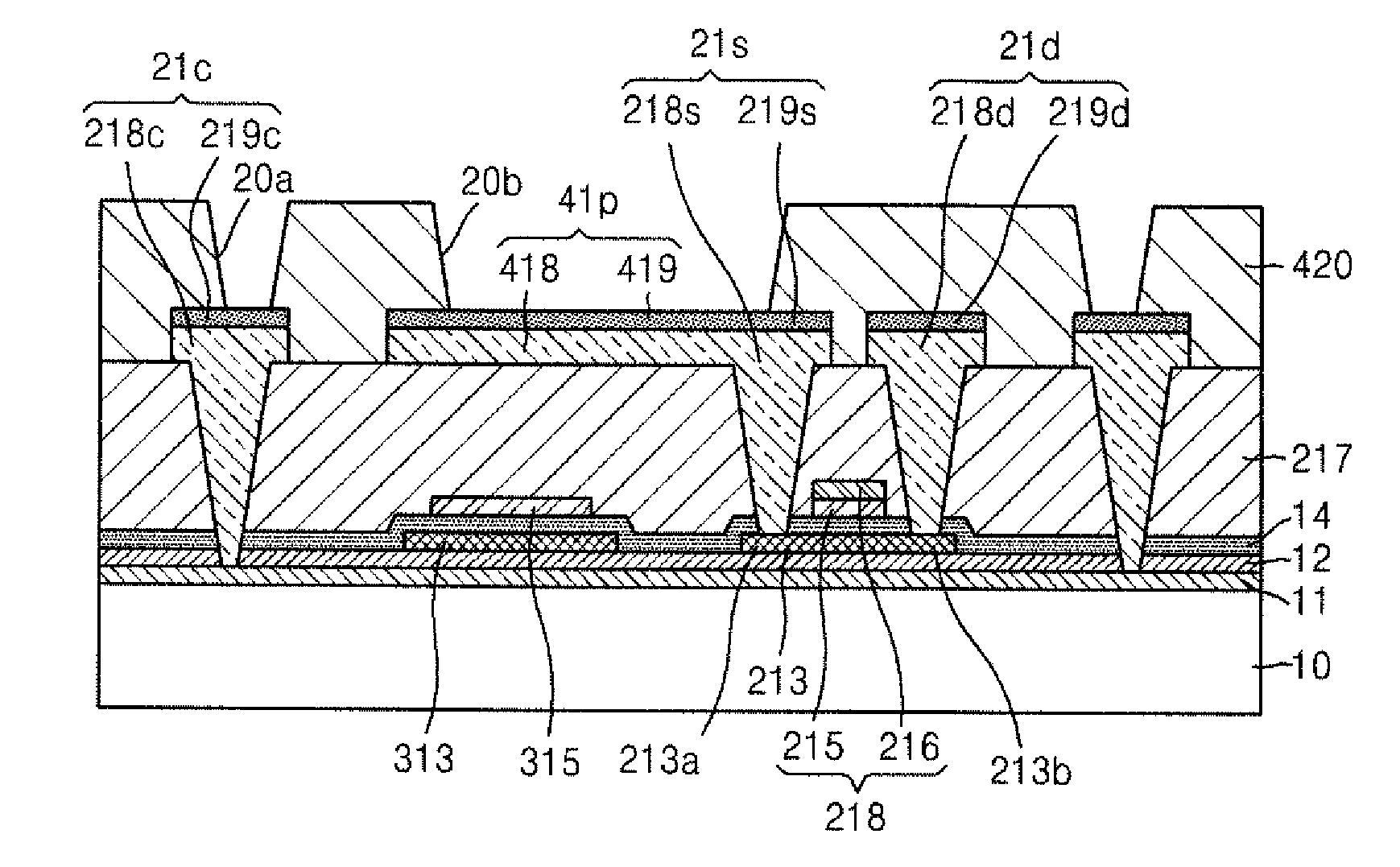
[0035]FIG. 1 is a cross-sectional view of an organic light-emitting display device according to an embodiment of the present invention.

[0036]Referring to FIG. 1, the organic light-emitting display device includes a substrate 10, a thin film transistor (TFT), a storage capacitor Cst, and an organic electroluminescent (EL) device.

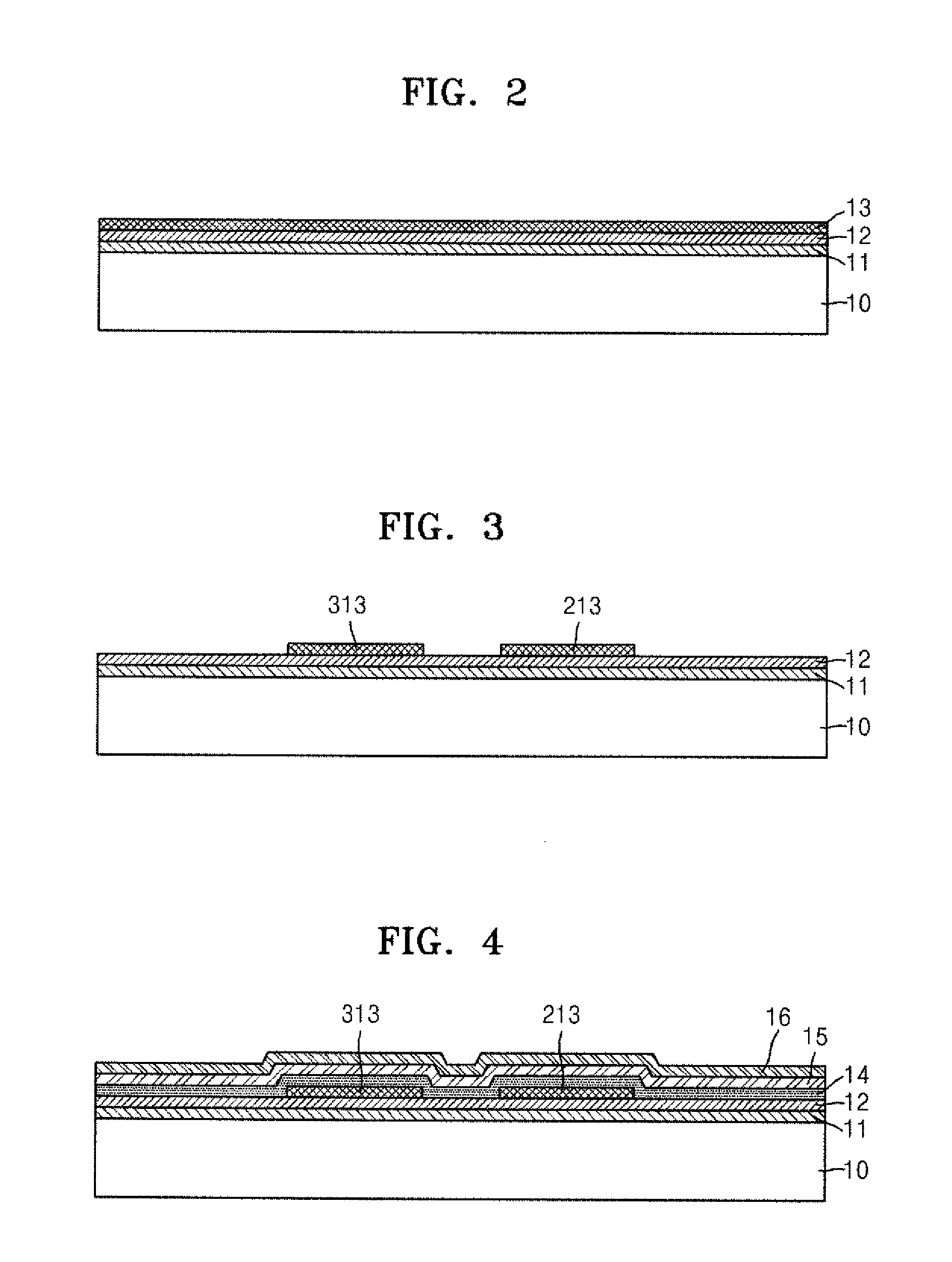
[0037]In more detail, an auxiliary electrode 11 is formed on the substrate 10, and a first insulating layer 12 including a buffer layer is formed on the auxiliary electrode 11. An active layer 213 of ...


PUM


Abstract

An organic light-emitting display device is manufactured via a simple process and has an improved aperture ratio. The organic light-emitting display device comprising: a substrate; an auxiliary electrode formed on the substrate; a thin film transistor (TFT) formed on the auxiliary electrode, the TFT comprising an active layer, a gate electrode, a source electrode and a drain electrode; an organic electroluminescent (EL) device electrically connected to the TFT and formed by sequentially stacking a pixel electrode formed on the same layer by using the same material as portions of the source and drain electrodes, an intermediate layer comprising an organic light emission layer (EML), and an opposite electrode disposed to face the pixel electrode; and a contact electrode formed on the same layer by a predetermined distance by using the same material as the source and drain electrodes, and electrically connecting the auxiliary electrode and the opposite electrode.

Description

CLAIM OF PRIORITY[0001]This application makes reference to, incorporates the same herein, and claims all benefits accruing under 35 U.S.C. §119 from an application earlier filed in the Korean Intellectual Property Office on 14 Dec. 2010 and there duly assigned Ser. No. 10-2010-0127857.BACKGROUND OF THE INVENTION[0002]1. Field of the Invention[0003]The present invention relates to an organic light-emitting display device and a method of manufacturing the same, and more particularly, to an organic light-emitting display device having an improved aperture ratio and a method of manufacturing the organic light-emitting display device.[0004]2. Description of the Related Art[0005]A flat panel display device, including an organic light-emitting display device, a liquid crystal display (LCD) device or the like, is manufactured on a substrate whereon a pattern including a thin film transistor (TFT), a capacitor, and a line including the TFT and the capacitor is formed.[0006]In general, in ord...

Claims


Application Information

Patent Timeline
Patent Type & Authority Applications(United States)
IPC IPC(8): H01L29/786
CPCH01L27/124H01L27/1255H01L2227/323H01L27/3279H01L27/3248H01L29/4908H10K59/123H10K59/1315H10K59/1201
Inventor YOU, CHUN-GICHOI, JOON-HOO
Owner SAMSUNG DISPLAY CO LTD
Why Eureka
Try Eureka