Organic electroluminescence display device manufacturing method and organic electroluminescence display device

a technology of electroluminescence display device and manufacturing method, which is applied in the direction of instruments, lighting and heating apparatus, sparking plugs, etc., can solve the problems of long time required for luminance measurement in the low gradation side, requiring time from the performance of luminance measurement for each pixel, etc., and achieves shortening of measurement tact, and shortening of luminance measurement tact

Inactive Publication Date: 2012-06-14
JOLED INC
View PDF4 Cites 20 Cited by
  • Summary
  • Abstract
  • Description
  • Claims
  • Application Information

AI Technical Summary

Benefits of technology

[0017]According to the present invention, it is possible to realize an organic EL display device and a manufacturing method thereof which can shorten the measuring tact, from when the luminance measurement for each pixel is performed up to when the correction parameter is obtained. Specifically, aside from being able to determine the external co...

Problems solved by technology

However, the conventional correction methods have the problems described below.
However, in the correction method which uses the least-square method for example, by nature it is necessary to perform the luminance measurement on each pixel for a number of gradation levels that is at least 3 gradation levels and preferably 5 gradation levels or more, and thus there is the problem of requiring time from the performance of the luminance measurement for each pixel up to the obtainment of the correction parameters.
In particular, a very long time is required for the luminance measurement in the low gradation-side.
As a result, there is the problem that measurement tact from the performance of the luminance measurement for each pixel up to the obtainment of the c...

Method used


Image

  • Organic electroluminescence display device manufacturing method and organic electroluminescence display device
  • Organic electroluminescence display device manufacturing method and organic electroluminescence display device
  • Organic electroluminescence display device manufacturing method and organic electroluminescence display device

Examples


embodiment

[0077]Hereinafter, an embodiment of the present invention shall be described with reference to the Drawings.

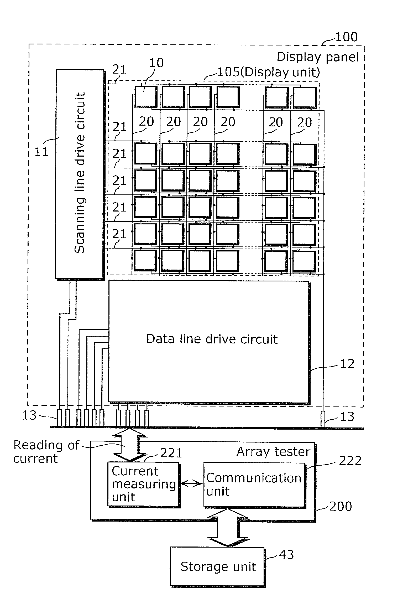
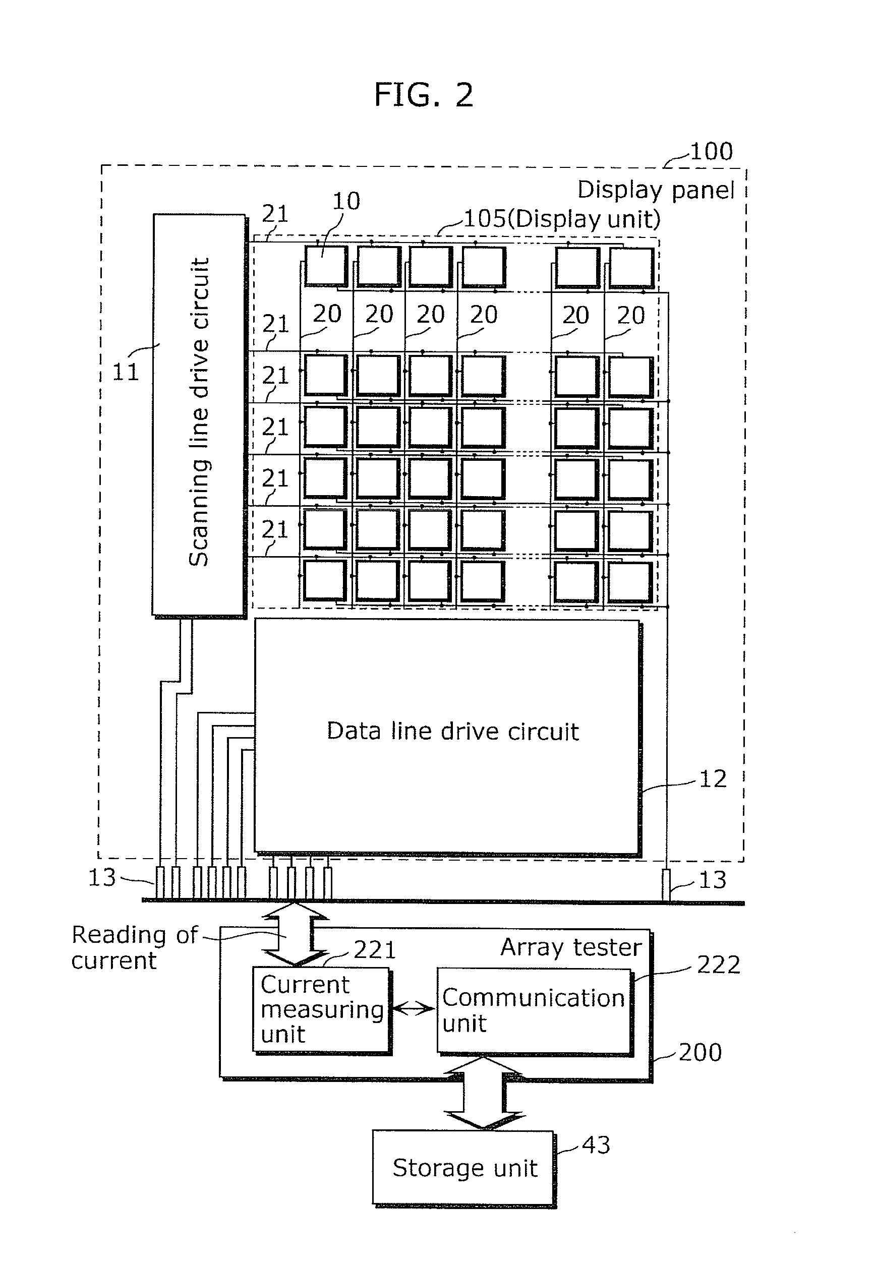
[0078]FIG. 2 is a block diagram showing a configuration of a forward circuit substrate assembled as a display panel and an array tester 200 which measures the circuit substrate. FIG. 3 is a diagram showing a circuit configuration of one pixel unit 10 included in a display unit 105.

[0079]The circuit substrate shown in FIG. 2 includes organic EL elements D1 and is assembled in a display panel 100 of an organic EL display device. The display unit 105, a scanning line drive circuit 11, a data line drive circuit 12, and input and output terminals 13 are formed on this circuit substrate.

[0080]The display unit 105 includes pixel units 10 which are arranged in m rows×n columns, and displays images based on an image signal which is a luminance signal inputted to the organic EL display device from an external source. Here, the circuit configuration of a pixel unit 10 shall be described ...


PUM


Abstract

A method of manufacturing an organic electroluminescence display includes preparing a substrate including pixels. The pixels each include a drive transistor and a capacitor. The capacitor of a subject pixel is caused to hold a voltage which corresponds to a threshold voltage of the drive transistor, and the voltage is read. A first signal voltage is obtained by adding a first correction parameter of the subject pixel to a second signal voltage corresponding to a single gradation level belonging to an intermediate gradation region or a high gradation region of representative voltage-luminance characteristics. The first signal voltage is applied to the driver of the subject pixel, and a luminance emitted by the subject pixel is measured. A second correction parameter with which the luminance emitted by the subject pixel becomes a standard luminance is calculated.

Description

CROSS REFERENCE TO RELATED APPLICATION[0001]This is a continuation application of PCT Application No. PCT / JP2010 / 002475 filed on Apr. 5, 2010, designating the United States of America, the disclosure of which, including the specification, drawings and claims, is incorporated herein by reference in its entirety.BACKGROUND OF THE INVENTION[0002]1. Field of the Invention[0003]The present invention relates to an organic electroluminescence (EL) display device manufacturing method and to an organic EL display device.[0004]2. Description of the Related Art[0005]Image display devices (organic EL displays) using organic electroluminescence elements (OLED: Organic Light-Emitting Diodes) are well-known as image display devices using current-driven light-emitting elements. Due to such advantages as excellent viewing angle characteristics and low power consumption, such organic EL displays have gained much attention as candidates for next-generation flat panel displays (FPDs).[0006]In organic E...

Claims


Application Information

Patent Timeline
IPC IPC(8): G09G3/32H01J9/42G09G5/10
CPCG09G3/006G09G3/3233G09G2300/0819G09G2300/0842G09G2360/16G09G2320/0233G09G2320/029G09G2320/0673G09G2360/145G09G2310/061H10K71/70H10K71/00
Inventor SEGAWA, YASUONAKAMURA, TETSUROUONO, SHINYA
Owner JOLED INC
Why Eureka
Try Eureka