Semiconductor chip and semiconductor package having the same

a semiconductor and chip technology, applied in the field of semiconductor packages, can solve the problems of fatigue fractures that may occur frequently in these connections, constant stress applied to the connections, and easy leakage of moisture to the connections, so as to improve the reliability of mounting

Inactive Publication Date: 2012-06-21
SK HYNIX INC
View PDF3 Cites 0 Cited by
  • Summary
  • Abstract
  • Description
  • Claims
  • Application Information

AI Technical Summary

Benefits of technology

[0010]An embodiment of the present invention is directed to a semiconductor chip capable of improving mounting reliability.

Problems solved by technology

However, the flip chip package encounters problems in that moisture is likely to leak to the connections and a stress is continuously applied to the connections due to a difference in CTE (coefficient of thermal expansion) between the semiconductor chip and the printed circuit board.
Accordingly, fatigue fracture may frequently occur in these connections.
However, the underfill process causes other problems in that it is difficult to control processing and voids are likely to be produced in the gap-fill substance.
Moreover, in the case where the underfill process is adopted, wetting may not be properly implemented in a subsequent process.
This may deteriorate processing stability and workability, thereby degrading the reliability and productivity of a flip chip package.
Nevertheless, in the event that the thickness of the film or the non-conductive adhesive is substantial, bumps of a semiconductor chip and a printed circuit board are likely to be improperly connected due to the substantial thickness of the film or the non-conductive adhesive, and a problem may result when transmitting electrical signals.

Method used


Image

  • Semiconductor chip and semiconductor package having the same
  • Semiconductor chip and semiconductor package having the same

Examples


Embodiment Construction

[0034]Hereafter, specific embodiments of the present invention will be described in detail with reference to the accompanying drawings. These exemplary embodiments of the invention are described with the understanding that the invention is not limited to these embodiments.

[0035]It is to be understood herein that the drawings are not necessarily to scale and in some instances proportions may have been exaggerated in order to more clearly depict certain features of the invention.

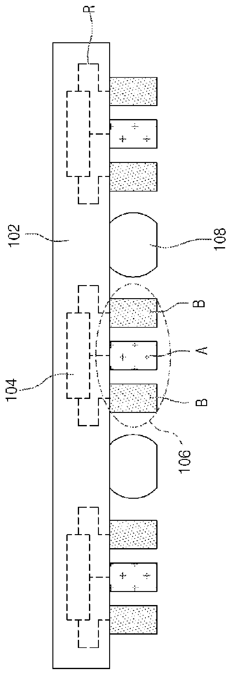
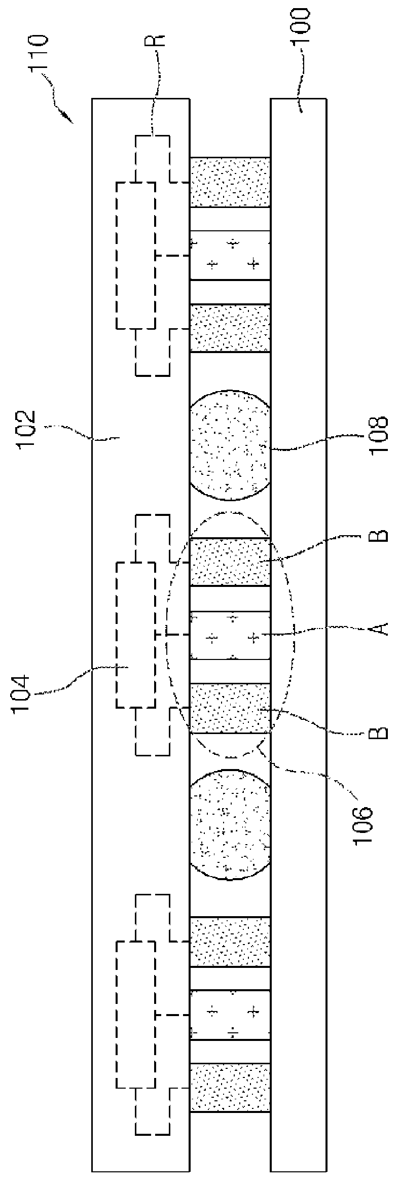
[0036]FIG. 1 is a cross-sectional view illustrating a semiconductor chip in accordance with an embodiment of the present invention.

[0037]Referring to FIG. 1, a semiconductor chip 110 in accordance with an embodiment of the present invention includes a semiconductor chip body 102, circuit patterns 104, connection members 108, and distance maintaining members 106.

[0038]The semiconductor chip body 102 may possess, for example, a rectangular hexahedral shape with a top surface and a bottom surface, with a pluralit...


PUM


Abstract

A semiconductor chip includes a semiconductor chip body having a first surface and a second surface that faces away from the first surface, and including a plurality of bonding pads disposed on the first surface. Also, the semiconductor chip includes a distance maintaining member attached to the first surface of the semiconductor chip body and electrically connected with a circuit pattern.

Description

CROSS-REFERENCE TO RELATED APPLICATIONS[0001]The present application claims priority to Korean patent application number 10-2010-0129868 filed on Dec. 17, 2010, which is incorporated herein by reference in its entirety.BACKGROUND OF THE INVENTION[0002]The present invention relates to a semiconductor package, and more particularly to a semiconductor chip with improved mounting reliability and a semiconductor package having the same.[0003]A flip chip package using bumps has been suggested to shorten electrical signal transfer paths between a semiconductor chip and a printed circuit board.[0004]The flip chip package has a structure in which a semiconductor chip is physically attached to and at the same time is electrically connected with a printed circuit board by bumps formed on bonding pads of the semiconductor chip. The flip chip package provides advantages in that, since electrical connections between the semiconductor chip and the printed circuit board are formed only by the bumps...

Claims


Application Information

Patent Timeline
Patent Type & Authority Applications(United States)
IPC IPC(8): H01L29/84
CPCH01L24/13H01L24/14H01L2924/07802H01L2224/16225H01L2924/3512H01L2224/131H01L2224/14515H01L24/16H01L24/17H01L24/81H01L2224/10122H01L2224/16227H01L2224/81007H01L2224/81191H01L2924/00015H01L21/563H01L2924/014H01L2924/00
Inventor HAN, KWON WHAN
Owner SK HYNIX INC
Why Eureka
Try Eureka