Capacitive touch panel

a capacitance touch panel and capacitance technology, applied in the field of capacitance touch panel, can solve the problems of false detection of input positions, affecting the enhancement of detection accuracy and size of touch panels, and increasing the size of circuit components, so as to increase the capacitance of the adjacent sensing electrodes, short time, and accurate detection of input positions

Inactive Publication Date: 2012-06-21
SMK CORP
View PDF3 Cites 23 Cited by
  • Summary
  • Abstract
  • Description
  • Claims
  • Application Information

AI Technical Summary

Benefits of technology

[0017]It is also an object of the invention to provide a capacitive touch panel with alternative arrangement of branch patterns of adjacent sensing electrodes, in which the capacitive touch panel reduces false detection by avoiding generation of a capacitive component due to crossing of lead wires.
[0034]The invention according to the fifth aspect causes the input unit to face the entire widths of branch patterns of adjacent sensing electrodes regardless of an input position. This reliably increases both the stray capacitances of the adjacent sensing electrodes, so that an input position between the sensing electrodes can be detected accurately.

Problems solved by technology

However, the increased number of sensing electrodes Ex arranged on the insulating substrate increases the frequencies of switching between the switches 101, 102, 104 and 105, leading to a longer time of detection and increased size of a circuit component.
Resultant size increase of a circuit component and a lengthened time of detection impose limits on the enhancement of detection accuracy and size increase of touch panels.
This may cause false detection of an input position depending on the size of the input unit or the location of the input position.
This generates new capacitive components at the crossings, leading to a fear of false detection and complicated wiring.

Method used


Image

  • Capacitive touch panel
  • Capacitive touch panel
  • Capacitive touch panel

Examples


Embodiment Construction

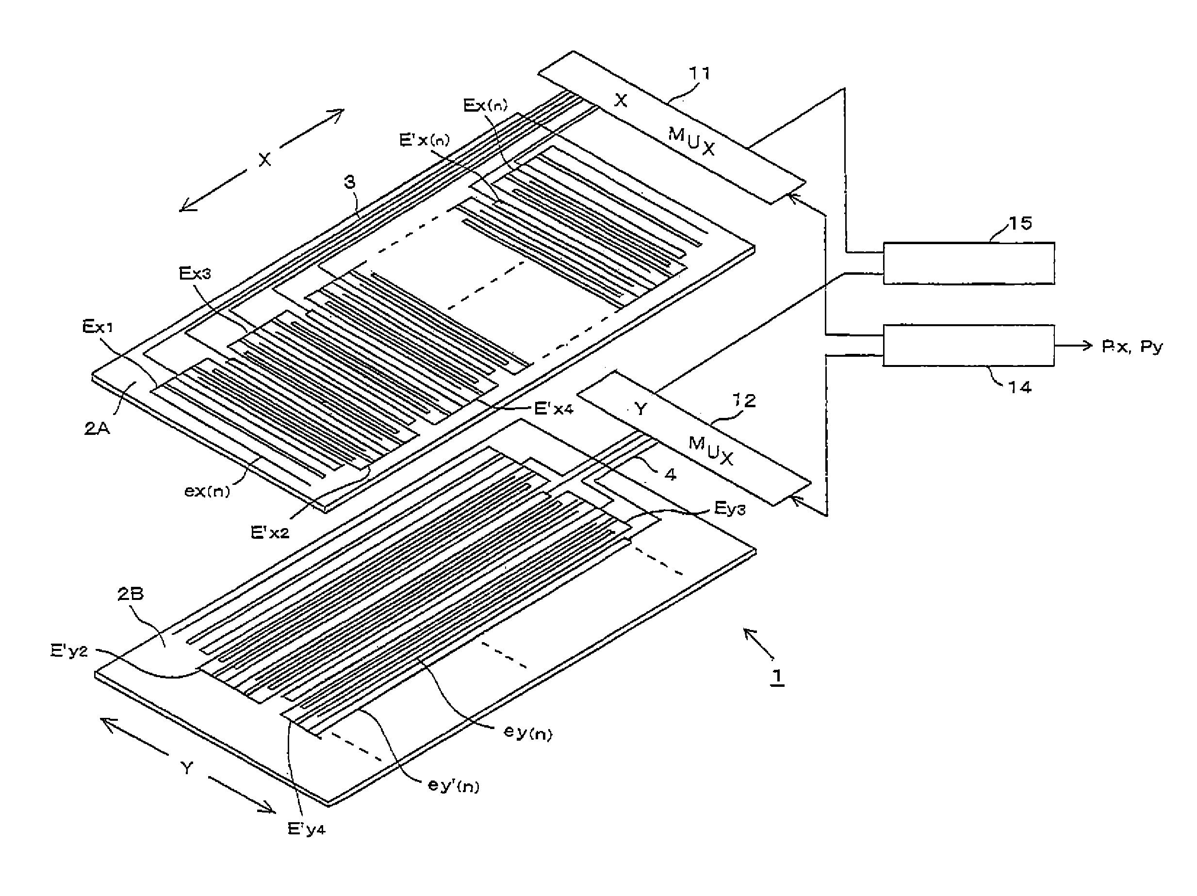
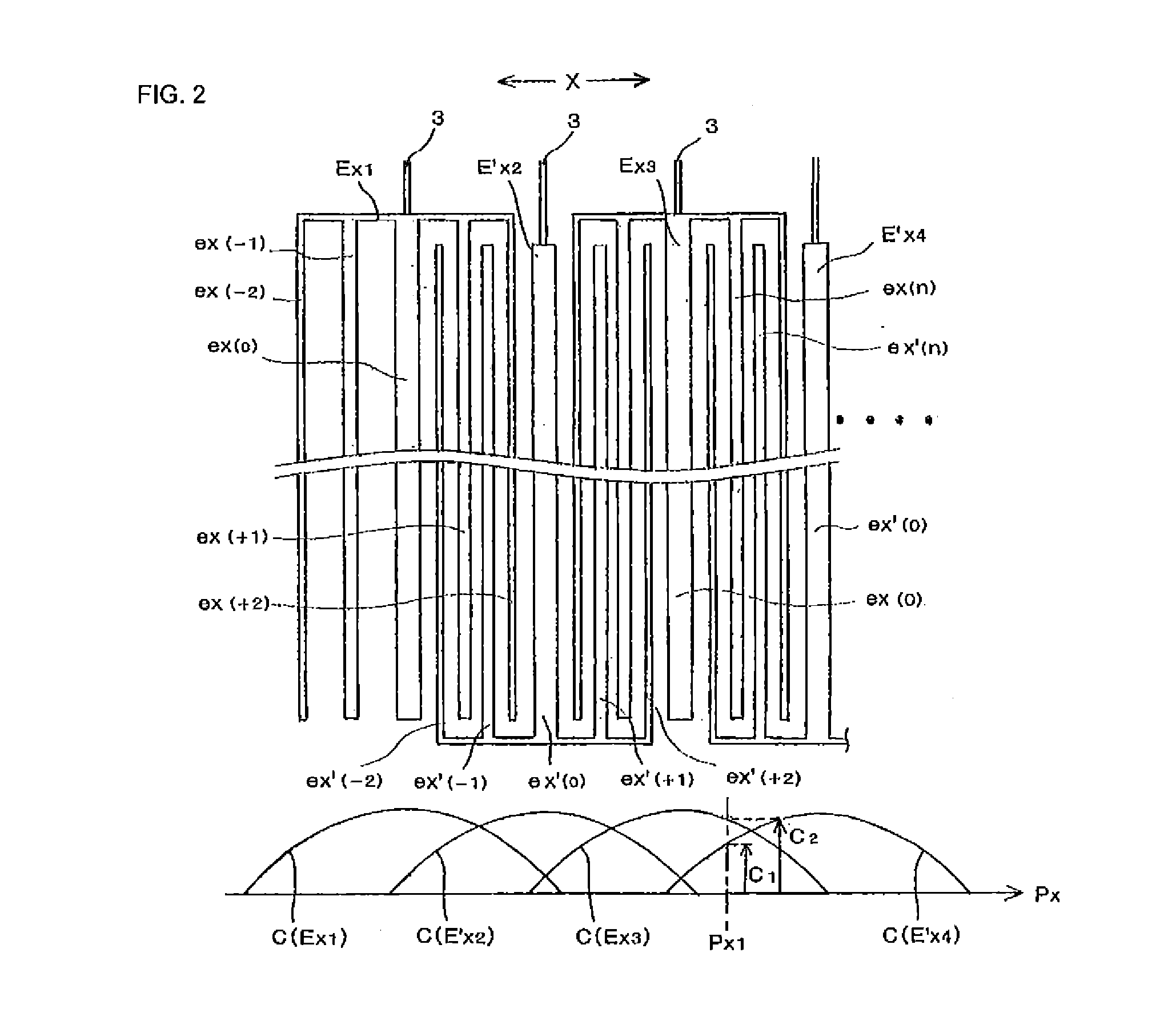
[0043]A capacitive touch panel 1 according to an embodiment of the invention will be described below with reference to FIGS. 1 to 5. When an input unit 10 such as a finger approaches a position on the capacitive touch panel 1, the capacitive touch panel 1 detects this position as an input position (Px, Py) in X and Y directions perpendicular to each other. As shown in FIG. 1, the capacitive touch panel 1 includes an insulating substrate 2A on which twenty nine (29) X sensing electrodes Ex and twenty nine (29) sensing electrodes Ex′ are arranged in the X direction with a predetermined pitch on a surface of the insulating substrate 2A, and an insulating substrate 2B on which sixteen (16) Y sensing electrodes Ey and sixteen (16) Y sensing electrodes Ey′ are arranged in a predetermined pitch on a surface of the insulating substrate 2B. The insulating substrates 2A and 2B are stacked one above the other.

[0044]Various materials such as flexible plastic sheets made of polyethylene terephth...


PUM


Abstract

A capacitive touch panel that detects an input position accurately with a limited number of sensing electrodes is provided. First and second sensing electrodes adjacent to each other in a detecting direction are arranged such that among a plurality of branch patterns of the first sensing electrode a branch pattern closer to the second sensing electrode, and among a plurality of branch patterns of the second sensing electrode a branch pattern closer to the first sensing electrode are alternately arranged in the detecting direction. The widths in the detecting direction of the plurality of branch patterns of each sensing electrode are set such that the branch patterns on the opposite sides in the detecting direction have the smallest width, and the width of a branch pattern gradually becomes greater as the branch pattern gets closer to a branch pattern at the center.

Description

CROSS-REFERENCE TO RELATED APPLICATIONS[0001]This application claims priority to Japanese Patent Application No. JP 2010-278861, filed Dec. 15, 2010. The entire contents of this application are hereby incorporated by reference herein.TECHNICAL FIELD[0002]The present invention relates to a capacitive touch panel that detects a sensing electrode to increase in stray capacitance in response to an input unit to make an input approaching the sensing electrode, and detects an input position on the basis of the location of the sensing electrode.BACKGROUND ART[0003]A capacitive touch panel is known as one of pointing devices for designating an item such as an icon displayed on a display of an electronic device, and making an input of the designated item. The capacitive touch panel detects an input position on an entry screen on the basis of the change of an electrostatic capacitance caused in response to an input unit such as a finger approaching a sensing electrode on the entry screen.[000...

Claims


Application Information

Patent Timeline
Patent Type & Authority Applications(United States)
IPC IPC(8): G06F3/045
CPCG06F3/044G06F3/0416G06F3/04166G06F3/0445G06F3/0446G06F3/0418
Inventor NAMBU, MOTOTOSHI
Owner SMK CORP
Why Eureka
Try Eureka