Method and apparatus for inspecting pattern defects

a pattern defect and inspection method technology, applied in the direction of instruments, spectrometry/spectrophotometry/monochromators, optical radiation measurement, etc., can solve the problems of difficult to find with certainty target defects that require product control, complicated lsi devices, and difficult to detect defects that are difficult for conventional technology to detect, so as to reduce the influence of an intensity, reduce the erroneous detection of grains, and detect various defects on the wafer stably

Inactive Publication Date: 2008-04-15
HITACHI HIGH-TECH CORP
View PDF12 Cites 22 Cited by
  • Summary
  • Abstract
  • Description
  • Claims
  • Application Information

AI Technical Summary

Benefits of technology

[0012]It is an object of the present invention to provide a method and apparatus capable of successfully detecting target defects in various processes by reducing erroneous detection of grains and morphology and by decreasing the influence of the intensity nonuniformity in interference light.
[0015]According to this invention, it becomes possible to reduce erroneous detection of grains and morphology, the decrease the influence of an intensity nonuniformity in interference light, and, thereby, to detect various defects on the wafer stably. These and other objects, features and advantages of the invention will be apparent from the following more particular description of preferred embodiments of the invention, as illustrated in the accompanying drawings.

Problems solved by technology

In particular, defects have been reported that are difficult for the conventional technology to detect, such as those referred to as “Non Visual Defects.”
LSI devices are becoming complicated and diversified in connection with the structures of inspection target patterns, such as in memory products formed mainly with repeating patterns and in logic products formed mainly with non-repeating patterns, and, consequently, it has become difficult to find with certainty target defects that require product control at the time of the manufacture of LSI devices. FIG. 2 shows an example of various target defects.
Target defects that are desired to be detected are voids and scratches produced in a CMP process, in addition to the presence of foreign materials and pattern defects produced in each process.
Moreover, there are short circuits and bridges in gate wiring in metal wiring parts, such as parts made of aluminum (Al), as well as non-conduction and non-aperture conditions of contact holes connecting the wiring.
Because underlayer patterns at locations where defects have occurred have become diversified, and due to the fact that the shape of a defect itself has been minimized (to dimensions equal to or less than the resolution of the conventional optical system) and diversified, it is difficult to detect many defects.
Moreover, in a process where a transparent film (here, meaning transparent to the illumination light), such as insulator film, is exposed at the outermost surface, an intensity nonuniformity in interference light due to minute film thickness differences of the transparent film appear as optical noise.
Therefore, there is a problem in that target defects whose dimensions are equal to or less than the resolution of the optical system are made apparent, while erroneous detection of a grain and morphology is lessened, and the influence of the intensity nonuniformity in interference light is reduced.
If the intensity ratio is changed in this way, the detected optical image will change in each measurement; therefore, there is a problem in that defect detection cannot be carried out stably.

Method used


Image

  • Method and apparatus for inspecting pattern defects
  • Method and apparatus for inspecting pattern defects
  • Method and apparatus for inspecting pattern defects

Examples


first embodiment

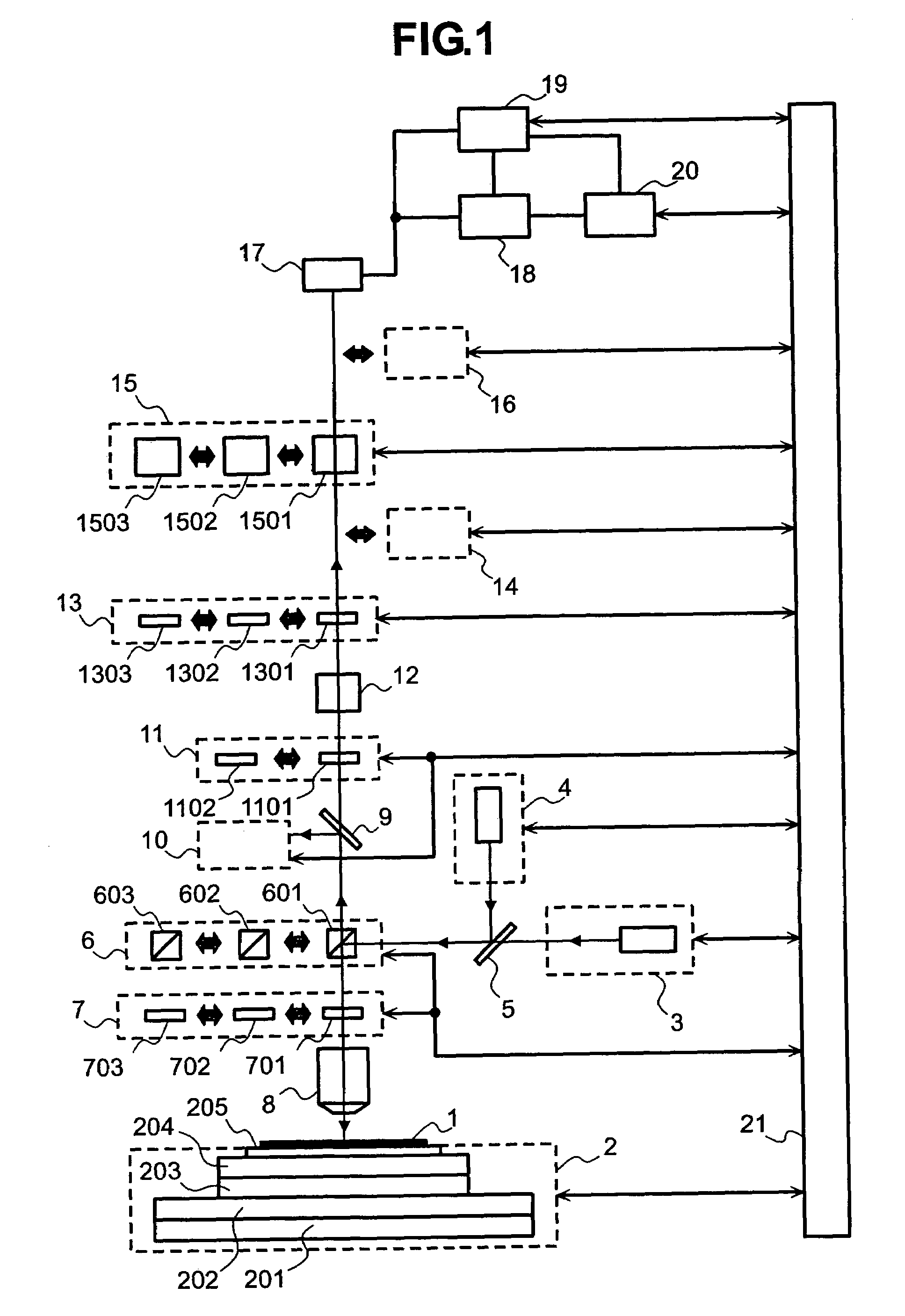
[0054]An embodiment in which an inspection apparatus according to this invention is applied to the inspection of a semiconductor device is shown in FIG. 1. The pattern defect inspection apparatus of this invention is composed of a conveyance system 2 for supporting and moving a wafer 1 that represents a target of inspection, illumination means 3 and 4 having different wavelengths, a dichroic mirror 5, a beam splitter (hereinafter referred to as BS) unit 6, a light modulation A unit 7, an objective lens 8, a BS for A / F 9, A / F detection unit 10, a light modulation B unit 11, a relay lens 12, a light modulation C unit 13, a pupil observation unit 14, an imaging lens unit 15, a sample surface observation unit 16, a light detector unit 17, a signal processing circuit 18, an auto classification (hereinafter referred to as ADC) unit 19, an input / output part 20, a controller 21 for these units, and an unillustrated relay lens and mirror. Here, arrows connecting the controller 21 and the var...

second embodiment

[0132]Another embodiment of the pattern defect inspection apparatus according to this invention is shown in FIG. 20. The pattern defect inspection apparatus of this invention is composed of: a conveyance system 2 that supports the inspection target wafer 1 and moves it, the illumination means 3 and 4 whose wavelengths are different, the BS units 22 and 23, the light modulation A unit 24, the objective lens 8, the A / F unit 25, the light modulation B unit 11, the relay lens 12, the light modulation C unit 13, the pupil observation unit 14, the imaging lens unit 15, the sample surface observation unit 16, the light detection unit 17, the signal processing circuit 18, the ADC unit 19, the input / output part 20, and an unillustrated controller, relay lens, and mirror.

[0133]This embodiment is different from the configuration explained in connection with Embodiment 1 in terms of the performance of the optical elements used in the BS units 22 and 23, the performance of the optical elements u...

third embodiment

[0140]Another embodiment of the pattern defect inspection apparatus according to this invention is shown in FIG. 24. The basic configuration of the pattern defect inspection apparatus of this embodiment is the same as that of Embodiment 1. This embodiment is constructed with a water injection system 26 and a drainage system 27, in addition to the configuration of Embodiment 1.

[0141]Next, details of the water injection system 26 and the drainage system 27 will be explained. The water injection system 26 has a function of supplying a medium 66 to a gap between the wafer 1 and the objective lens 8, and the drainage system 27 has a function of removing the medium 66 supplied to the gap between the wafer 1 and the objective lens 8. Here, the medium 66 has a refractive index that is larger than that of air (12 etc. at the illumination wavelength) and causes no damage to the wafer 1. For example, this may be pure water as regularly used in semiconductor factories.

[0142]The object of this e...


PUM

PropertyMeasurementUnit
wavelengthaaaaaaaaaa

Abstract

A method of inspecting pattern defects can detect target defects in various processes stably by reducing erroneous detection of grains and morphology and decreasing the influence of an intensity nonuniformity in interference light. For this purpose, lights emitted from two sources of illumination capable of outputting a plurality of wavelengths are reflected by a beam splitter and irradiated onto a wafer. Diffracted light from the wafer is converged by an objective lens, is made to pass through light modulation units and imaged on an image sensor in a light detection unit. Then, defects are detected in a signal processing unit. Further, the optical modulation unit is made to have a structure that uses a plurality of optical components selectively and which can be optimized according to target defects.

Description

BACKGROUND OF THE INVENTION[0001]The present invention relates in general to pattern defect inspection and foreign material inspection for detecting defects (short circuits, breaking of wire, etc.) in a circuit pattern and foreign materials on a sample; and, more particularly, the invention relates to a method and apparatus for inspecting for defects and foreign materials on a circuit pattern, such as those which appear in semiconductor wafers, liquid crystal displays, photomasks, etc. In the following description, a defect includes the presence of foreign material.[0002]Conventionally, as an example of an inspection apparatus of this kind, there is a technology in which an image of a sample is picked up using an imager, such as an image sensor, while the sample is being moved, and gray scales of the detected image signal and of an image signal that has been delayed for a fixed time are compared, whereby a portion where the two signals do not coincide is identified as a defect (JP-A...

Claims


Application Information

Patent Timeline
Patent Type & Authority Patents(United States)
IPC IPC(8): G01N21/00
CPCG01N21/95G01N2021/9513
Inventor NISHIYAMA, HIDETOSHISHIBATA, YUKIHIROMAEDA, SHUNJIYOSHIDA, MINORU
Owner HITACHI HIGH-TECH CORP
Why Eureka
Try Eureka