


Quick Research
Generate reliable direction feasibility study reports for your R&D in just a few steps.

Technical Q&A
Discover and master advanced knowledge NOW. Basics, ideas, possibilities, all at once.

Find Solutions
As an expert in R&D theories, this can generate solutions to your technical problems instantly.

Evaluate Feasibility
Analyze your overall solution with one click, know your potential R&D risks in advance.

Monitor Landscape
Get weekly tech updates, stay abreast of the latest tech innovations and key insights.
Leadless semiconductor package and method of manufacture
a technology of semiconductor packaging and leadframe, which is applied in the direction of semiconductor devices, semiconductor/solid-state device details, line/current collector details, etc., can solve the problem that the thickness requirement of leadframe strips cannot be much less than 100 m, and the thickness of leadframe strips is virtually impossible to handle without damag
- Summary
- Abstract
- Description
- Claims
- Application Information
AI Technical Summary
Problems solved by technology
Method used
Image

Examples
Embodiment Construction
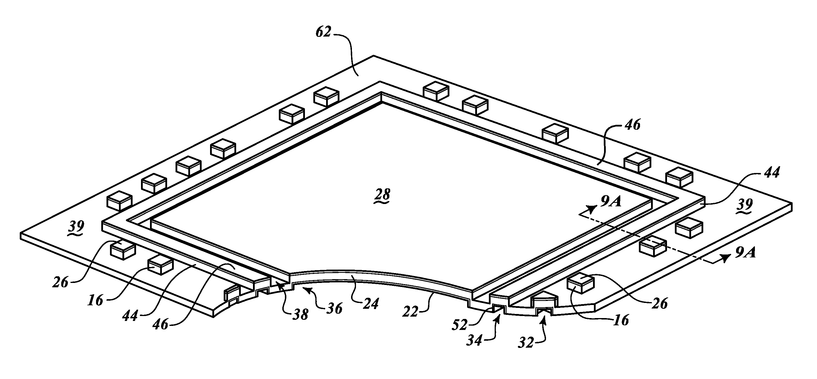
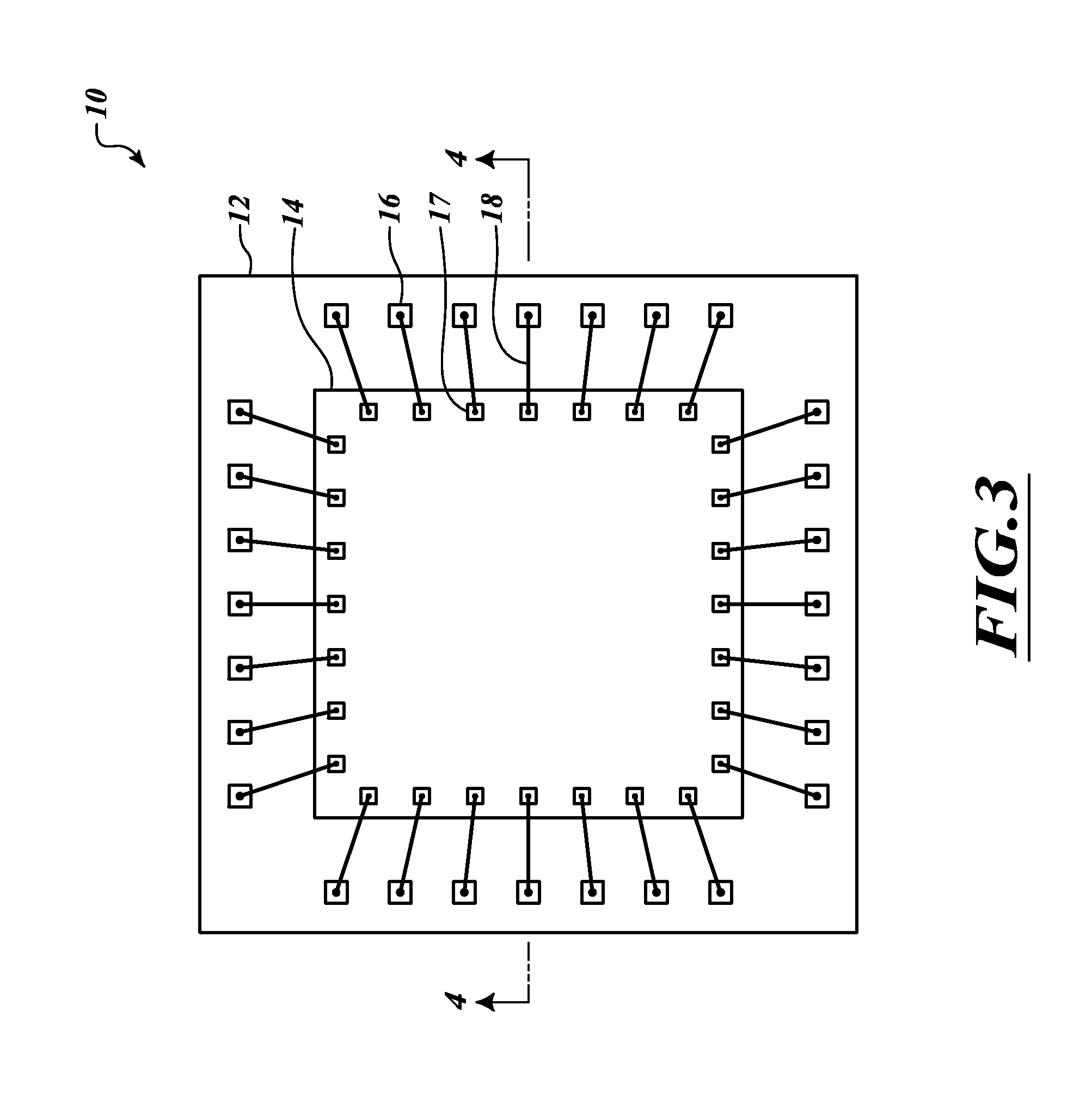
[0022]Turning now to FIG. 3, a plan view is provided of a leadframe-based semiconductor package 10 according to an embodiment. The package 10 is encapsulated in a molding compound body 12 that is shown as though transparent in order to show the internal structure. The package 10 is in a quad flat pack, no lead (QFN) configuration, and includes a semiconductor die 14 with a plurality of contact pads 17, a plurality of bond pads 16, and a plurality of bond wires 18 coupled between respective pairs of the bond pads and the contact pads.
[0023]FIG. 4 is a cross-sectional view of the semiconductor package 10 taken along lines 4-4 of FIG. 3. Portions of a leadframe 21 are visible, including a die paddle 24 on which the semiconductor die 14 is mounted, and also including a plurality of bond pads 16. The die paddle 24 and bond pads 26 are formed from a common sheet of metal, preferably copper or a copper alloy. An upper plating 26 and a lower plating 22 are positioned on each of the bond pad...
PUM
| Property | Measurement | Unit |
|---|---|---|
| Length | aaaaa | aaaaa |
| Length | aaaaa | aaaaa |
| Length | aaaaa | aaaaa |
Abstract
Description
Claims
Application Information
 - R&D Engineer
- R&D Manager
- IP Professional
- Industry Leading Data Capabilities
- Powerful AI technology
- Patent DNA Extraction
Browse by: Latest US Patents, China's latest patents, Technical Efficacy Thesaurus, Application Domain, Technology Topic, Popular Technical Reports.
© 2024 PatSnap. All rights reserved.Legal|Privacy policy|Modern Slavery Act Transparency Statement|Sitemap|About US| Contact US: help@patsnap.com