Liquid-crystal panel and liquid-crystal display device

a liquid crystal display and panel technology, applied in non-linear optics, instruments, optics, etc., can solve the problem of undetectable complex manufacturing steps of mva mode, and achieve the effect of simple manufacturing steps, improved viewing angle characteristics, and excellent viewing angle characteristics

Inactive Publication Date: 2012-07-05
SHARP KK
View PDF3 Cites 25 Cited by
  • Summary
  • Abstract
  • Description
  • Claims
  • Application Information

AI Technical Summary

Benefits of technology

[0026]A liquid crystal panel and a liquid crystal panel according to the present invention are each configured such that in such a vertical alignment liquid crystal panel based on a transverse electric field drive system, at least one of the first and second substrates is provided with an insulating layer, and those regions of the insulating layer (first insulating layer) which correspond to the blue, green, and red subpixels have the relative permittivities specified above, respectively; therefore, a tone reversal can be prevented and, moreover, VT (voltage-transmittance) curves obtained in the blue, green, and red subpixels can be made similar in shape to one another. For this reason, the present invention makes it possible to provide a liquid crystal panel that shows few changes in color as observed when the liquid crystal panel is looked squarely at.
[0027]Further, in a case where the liquid crystal panel includes, in each pixel, at least two regions of the insulating layer (first insulating layer) that are different in relative permittivity from each other, at least two regions that are different in shape of equipotential lines from each other are formed in each pixel when the transverse electric field is generated. Since, in this case, at least two regions that are different in alignment direction of liquid crystal molecules from each other are formed in each pixel, regions having different VT curves can be formed in each pixel. This makes it possible, as a result, to subject the liquid crystal panel to VT multiplication and improve the viewing angle characteristic of the liquid crystal panel.
[0028]Therefore, as described above, in case where the liquid crystal panel includes, in each pixel, at least two regions of the insulating layer (first insulating layer) that are different in relative permittivity from each other, a liquid crystal panel can be provided which shows few changes in color when looked squarely at, which has an excellent viewing angle characteristic, and which can be manufactured through simple steps.

Problems solved by technology

However, the MVA mode undesirably requires complex manufacturing steps.

Method used


Image

  • Liquid-crystal panel and liquid-crystal display device
  • Liquid-crystal panel and liquid-crystal display device
  • Liquid-crystal panel and liquid-crystal display device

Examples


embodiment 1

[0124]An embodiment of the present invention is described below with reference to FIGS. 1 through 20.

[0125]First, a configuration of a liquid crystal panel according to the present embodiment and a configuration of a liquid crystal display device according to the present embodiment are schematically described below.

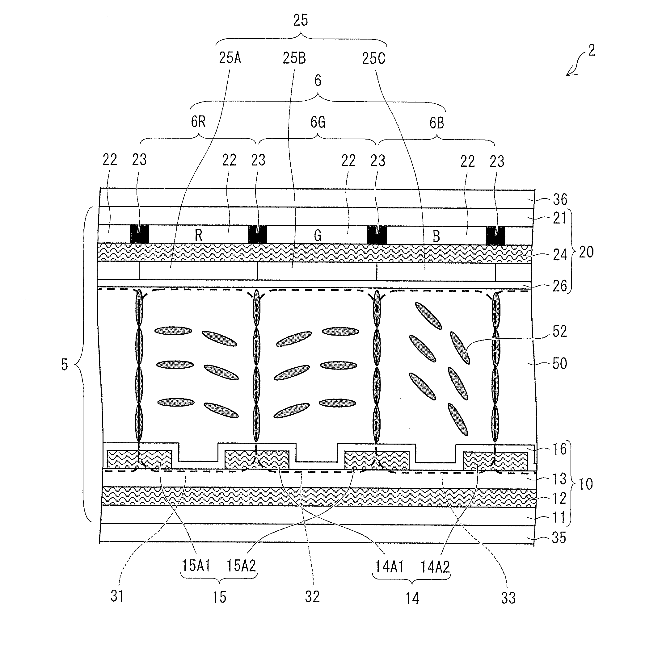
[0126]FIG. 3 is a cross-sectional view schematically showing a configuration of a liquid crystal display device according to the present embodiment.

[0127]As shown in FIG. 3, a liquid crystal display device 1 according to the present embodiment includes a liquid crystal panel 2 (liquid crystal display panel, liquid crystal display element), a driving circuit 3, and a backlight 4 (lighting device). The driving circuit 3 and the backlight 4 are configured in the same manners as their conventional counterparts. Therefore, their configurations are not described below.

[0128]FIG. 1 is a cross-sectional view schematically showing a configuration of a main part of the liquid cryst...

embodiment 2

[0367]Another embodiment of the present invention is described below with reference to FIGS. 21 and 22.

[0368]It should be noted that the following description mainly explains points of difference from the liquid crystal panel 2 according to Embodiment 1. Those components having the same functions as those described above in Embodiment 1 are given the same reference numerals, and as such, are not described below.

[0369]FIG. 21 is a cross-sectional view schematically showing a configuration of a main part of a liquid crystal panel 2 according to the present embodiment.

[0370]As shown in FIG. 21, the liquid crystal panel 2 according to the present embodiment differs from the liquid crystal panel 2 shown in FIG. 1 in that the substrate 10 is replaced by a substrate 60 not provided with a solid electrode 12 or an insulating layer 13 serving as an array-side insulating layer. That is, the liquid crystal panel 2 of the present embodiment does not have an FFS structure.

[0371]The substrate 60 ...

embodiment 3

[0392]Still another embodiment of the present invention is described below with reference to FIGS. 23 and 24.

[0393]It should be noted that the following description mainly explains points of difference from the liquid crystal panel 2 according to Embodiment 1. Those components having the same functions as those described above in Embodiments 1 and 2 are given the same reference numerals, and as such, are not described below.

[0394]FIG. 23 is a cross-sectional view schematically showing a configuration of a main part of a liquid crystal panel 2 according to the present embodiment.

[0395]As shown in FIG. 23, the liquid crystal panel 2 according to the present embodiment includes a substrate 80 (array substrate), a substrate 70 (counter substrate), and a liquid crystal layer 50 sandwiched between the substrate 80 and the substrate 70.

[0396]As shown in FIG. 23, the substrate 80 includes: a glass substrate 11; a solid electrode 12 (third electrode) stacked on the glass substrate 11; an ins...


PUM

PropertyMeasurementUnit
relative permittivityaaaaaaaaaa

Abstract

A vertical alignment liquid crystal panel based on a transverse electric field drive system is provided which shows few changes in color when looked squarely at. A liquid crystal panel (2) is a vertical alignment liquid crystal panel based on a transverse electric field drive system, which carries out a display by driving, with a transverse electric field, a liquid crystal layer (50) sandwiched between substrates (10, 20), and the substrate (10) is provided with an insulating layer (25) having at least two regions that are different in relative permittivity from each other in a pixel (6) composed of a red subpixel (6R), a green subpixel (6G), and a blue subpixel (6B). Those regions of the insulating layer (25) which correspond to the blue, green, and red subpixel (6B, 6G, 6R) in the liquid crystal panel (2) have relative permittivities of 3, 3 to 7, and 4 to 7, respectively.

Description

TECHNICAL FIELD[0001]The present invention relates to liquid crystal panels and liquid crystal display devices and, more specifically, to (i) a liquid crystal panel in which transmission of light is controlled by applying a transverse electric field to a vertical alignment liquid crystal cell whose liquid crystal molecules are aligned along a direction perpendicular to the substrates when no voltage is applied and (ii) a liquid crystal display device including such a liquid crystal panel.BACKGROUND ART[0002]Among various display devices, liquid crystal display devices have such advantages as thinness, light weight, and low power consumption. For this reason, in recent years, liquid crystal display devices have been widely used instead of CRTs (cathode-ray tubes) in various fields of TVs (televisions), monitors, mobile devices such as cellular phones, etc.[0003]A liquid crystal display device has its display system determined according to the way in which the liquid crystals are alig...

Claims


Application Information

Patent Timeline
Patent Type & Authority Applications(United States)
IPC IPC(8): G02F1/1333
CPCG02F1/133345G02F1/134363G02F2001/133742G02F1/133514G02F1/1393G02F1/133742
Inventor MURATA, MITSUHIROKOZAKI, SHUICHIISHIHARA, SHOICHISAKURAI, TAKEHISAOHTAKE, TADASHI
Owner SHARP KK
Why Eureka
Try Eureka