Manufacturing of electronic components

a technology of electronic components and manufacturing methods, applied in the direction of liquid surface applicators, coatings, semiconductor devices, etc., can solve the problems that integrated circuit based electronics are not optimal for all applications

Active Publication Date: 2012-07-12
SMARTRAC INVESTMENT BV
View PDF1 Cites 0 Cited by
  • Summary
  • Abstract
  • Description
  • Claims
  • Application Information

AI Technical Summary

Benefits of technology

[0009]According to an embodiment, the cross-sectional area of the third portion is less than the cross-sectional area of the first portion and the cross-sectional area of the second portio...

Problems solved by technology

However, integrated circuit based elec...

Method used


Image

  • Manufacturing of electronic components
  • Manufacturing of electronic components
  • Manufacturing of electronic components

Examples


Embodiment Construction

[0021]Although the specification may refer to “an”, “one”, or “some” embodiment(s) in several locations, this does not necessarily mean that each such reference is to the same embodiment(s), or that the feature only applies to a single embodiment. Single features of different embodiments may also be combined to provide other embodiments.

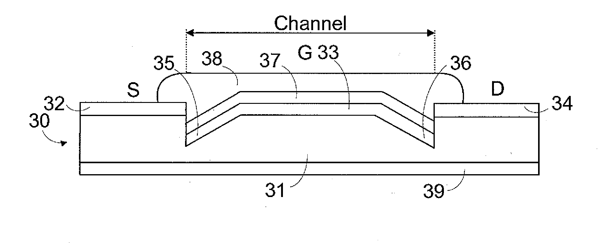
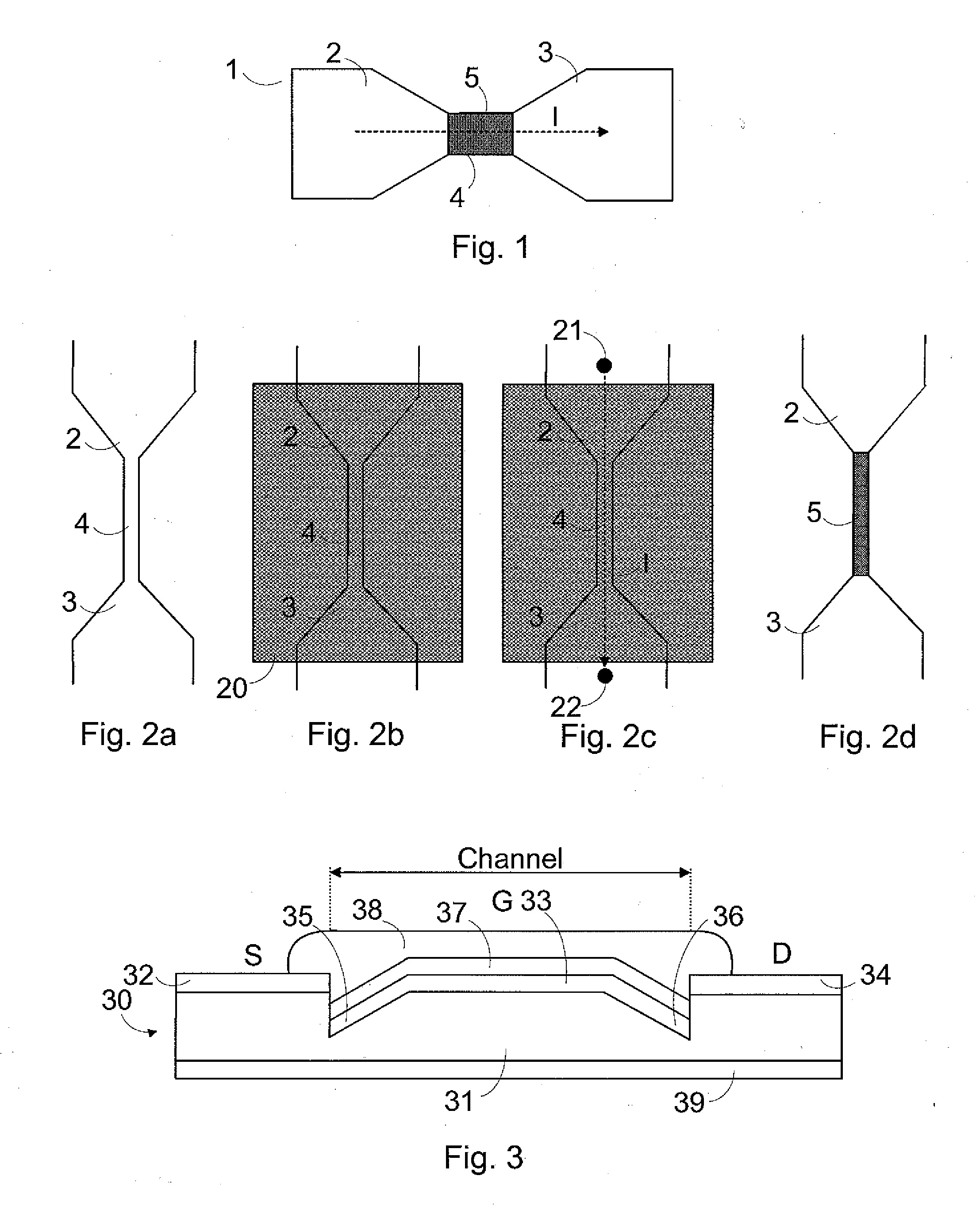
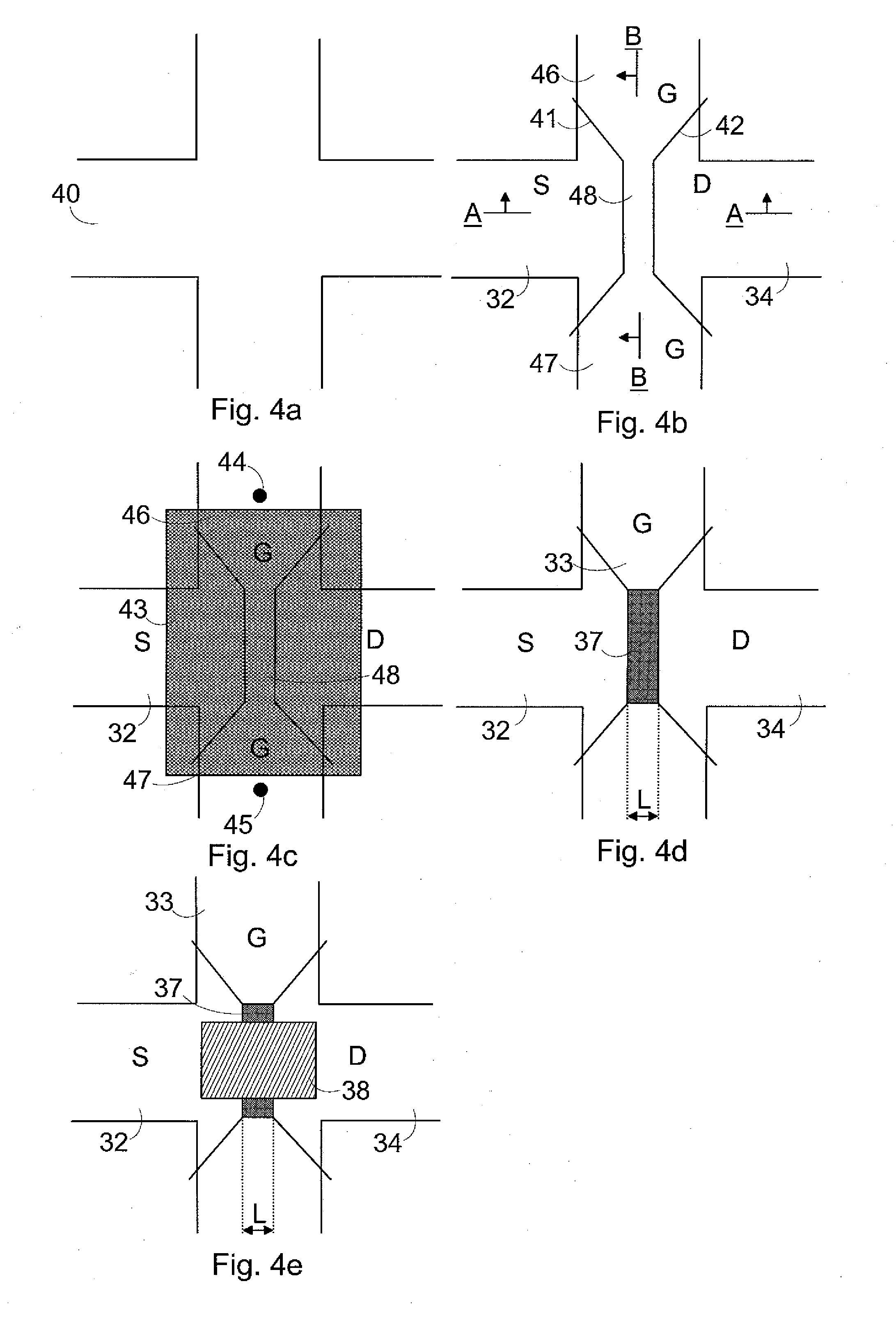
[0022]FIG. 1 illustrates a simplified top-view of an electronic component 1. The component comprises a conducting element comprising a first portion 2, a second portion 3 and a third portion 4 between the first portion 2 and the second portion 3. The third portion 4 is narrower, i.e. the cross-sectional area of the third portion 4 is less than the cross-sectional areas of the first portion 2 and the second portion 3. It is to be noted that the third portion 4 may additionally or instead be thinner than the first portion 2 and the second portion 3 from a side-view of the electronic component 1.

[0023]The electronic component could be a thin-film compon...


PUM


Abstract

According to an aspect of the invention, a method is provided for manufacturing electronic components. A conducting element comprising a first portion, a second portion and a third portion between the first portion and the second portion is provided. Thermally responsive dielectric material is added at least onto the third portion of the conducting element. Electric current is supplied between the first portion and the second portion of the conducting element causing ohmic heating to affix dielectric material located on the third portion to the third portion. Non-thermally-affixed dielectric material is removed.

Description

FIELD [0001]The invention relates to embossing electronic components, and in particular to arranging dielectric material on top of a conductive element.BACKGROUND [0002]Modern integrated circuits, typically silicon based structures, have very high integration density. As one descriptive parameter of this, the number of transistors per given surface area is growing steadily. However, integrated circuit based electronics are not optimal for all applications. For some applications, the integration density and / or speed of the electronics is less crucial. Therefore, for certain applications, different types of printable electronics are becoming more and more interesting.[0003]One approach to reducing transistor cost, while still maintaining acceptable performance, is to produce thin-film transistors on a suitable substrate by printing. Here printing means that at least some device layers have been manufactured by printing techniques. There are several known ways of manufacturing basic co...

Claims


Application Information

Patent Timeline
IPC IPC(8): H01L51/10B05C21/00H01L51/40
CPCH01L51/0023H01L2251/105H01L51/0545H01L51/052H10K71/621H10K10/471H10K10/466H10K71/821
Inventor BACKLUND, TOMASLILJA, KAISAJOUTSENOJA, TIMO
Owner SMARTRAC INVESTMENT BV
Why Eureka
Try Eureka