MEMS device assembly and method of packaging same

a technology of microelectromechanical systems and devices, applied in the direction of instruments, loudspeakers, fluid pressure measurement, etc., can solve the problems of high thermally induced stress that can develop during the manufacture of mems devices, output shifts in mems devices, and instability of mems devices

Inactive Publication Date: 2012-07-12
NORTH STAR INNOVATIONS
View PDF1 Cites 22 Cited by
  • Summary
  • Abstract
  • Description
  • Claims
  • Application Information

AI Technical Summary

Problems solved by technology

There are significant challenges to be surmounted in the packaging of MEMS devices due at least in part to the necessity for the MEMS devices to interact with the outside environment, the fragility of many types of MEMS devices, and severe cost constraints.
As such, a high thermally induced stress can develop during MEMS device manufacture or operation.
Variations in package stress can cause instability of the MEMS device and output shifts in the MEMS device.

Method used


Image

  • MEMS device assembly and method of packaging same
  • MEMS device assembly and method of packaging same
  • MEMS device assembly and method of packaging same

Examples


Embodiment Construction

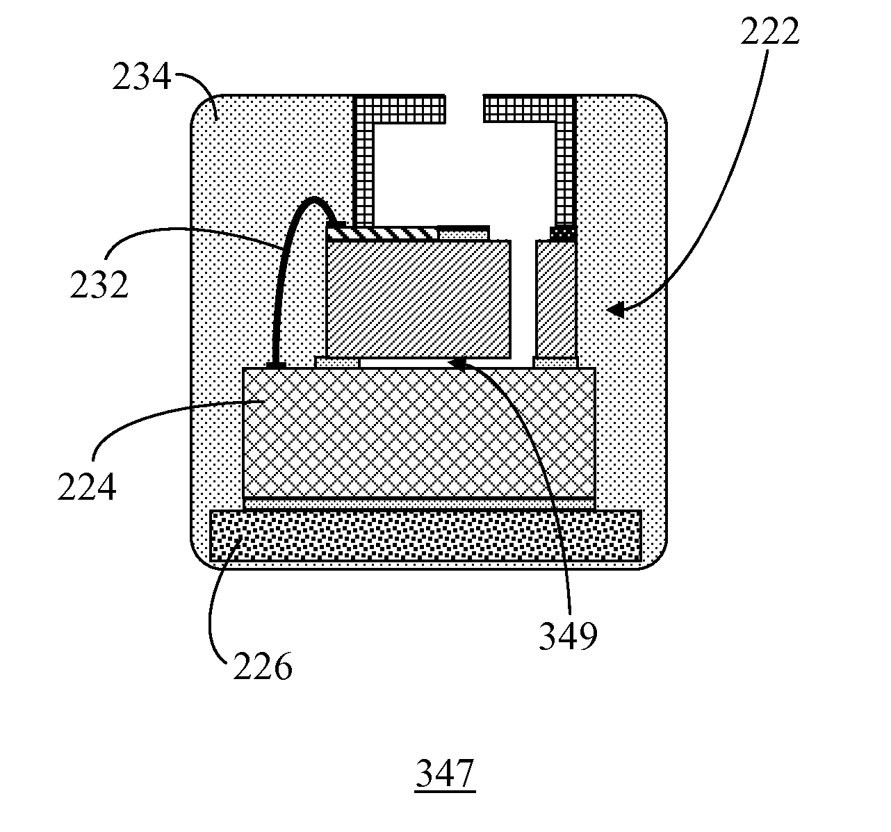
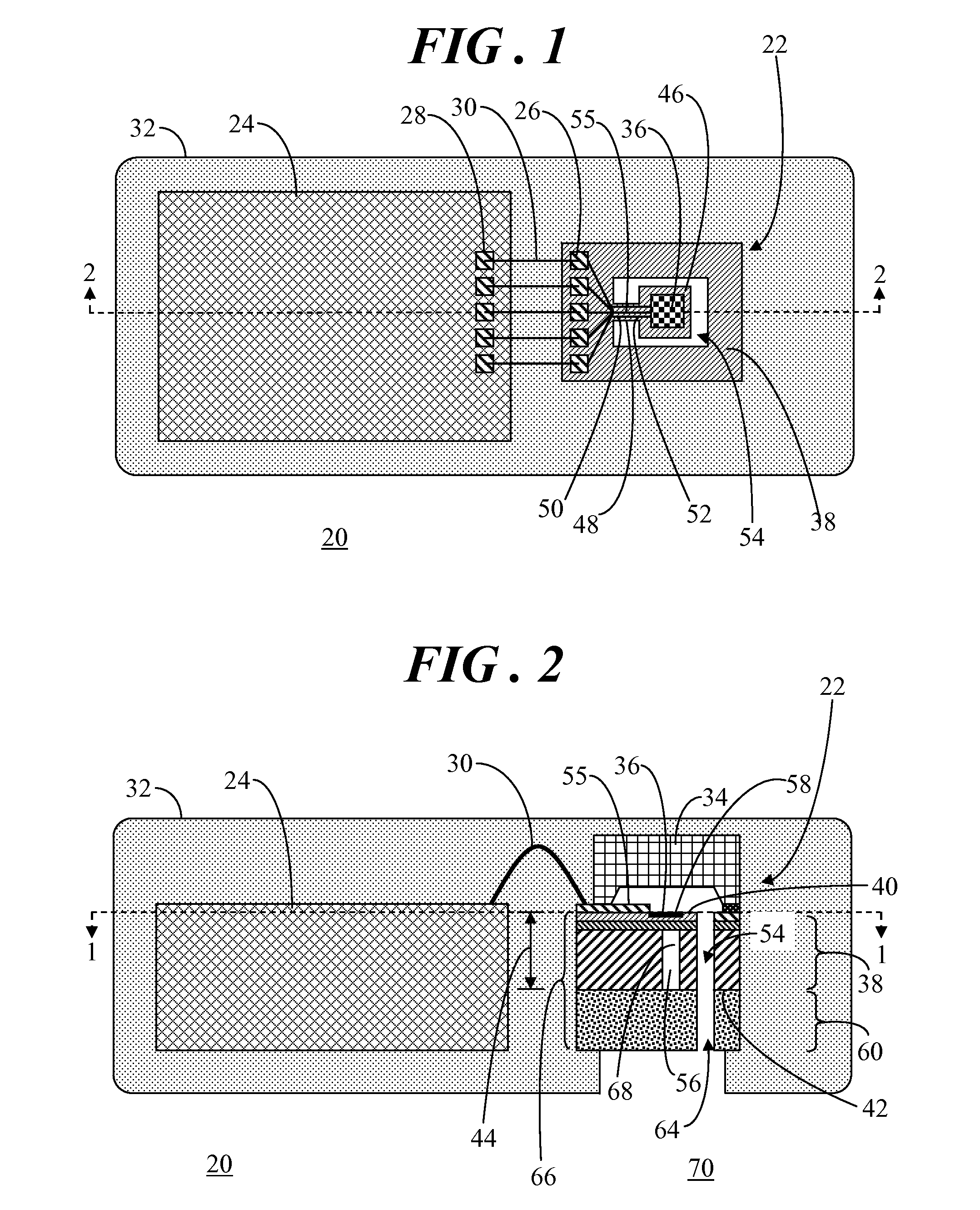
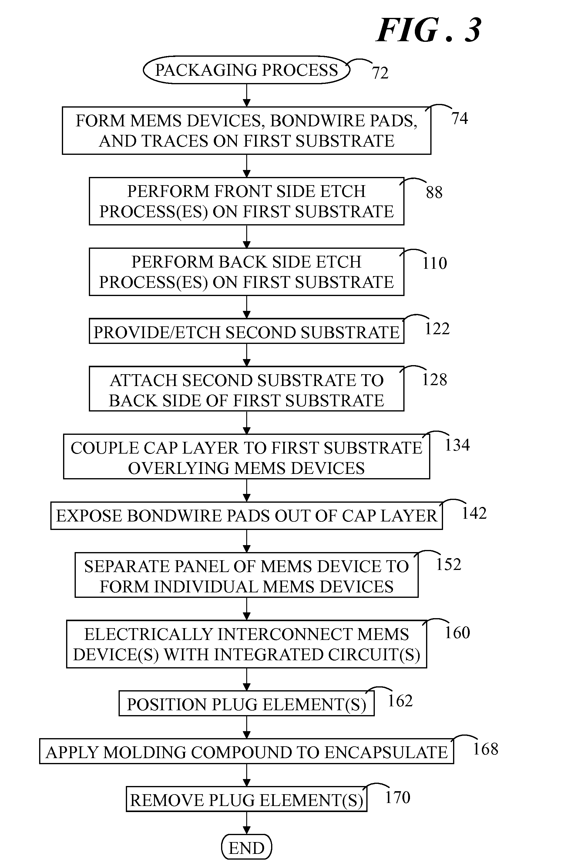
[0037]As the uses for MEMS devices continue to grow and diversify, increasing emphasis is being placed on smaller size and low cost packaging without sacrificing part performance. Another continuing challenge in MEMS device packaging is providing environmental protection for the fragile moving parts of a MEMS device that does not affect the mechanical motion of these moving parts. Embodiments entail microelectromechanical systems (MEMS) device assemblies and a method of packaging such MEMS device assemblies for improved stress isolation. In particular, MEMS devices are created through the execution of relatively simple methodology as cantilevered structures that provide improved package stress isolation. The methodology additionally allows for the use of low-cost overmolded packaging that provides the appropriate environmental protection of the MEMS devices without affecting the mechanical motion of the moving parts of the MEMS devices.

[0038]Referring now to FIGS. 1 and 2, FIG. 1 sh...


PUM


Abstract

An assembly (220) includes a MEMS die (222) and an integrated circuit (IC) die (224) attached to a substrate (226). The MEMS die (222) includes a MEMS device (237) formed on a substrate (242). A packaging process (264) entails forming the MEMS device (237) on the substrate (242) and removing a material portion of the substrate (237) surrounding the device (237) to form a cantilevered substrate platform (246) suspended above the substrate (226) at which the MEMS device (237) resides. The MEMS die (222) is electrically interconnected with the IC die (224). A plug element (314) can be positioned overlying the platform (246). Molding compound (32) is applied to encapsulate the die (222), the IC die (224), and substrate (226). Following encapsulation, the plug element (314) can be removed, and a cap (236) can be coupled to the substrate (242) overlying an active region (244) of the MEMS device (237).

Description

RELATED INVENTION[0001]The present invention is a continuation in part (CIP) of “MEMS Device Assembly and Method of Packaging Same,” U.S. patent application Ser. No. 12 / 873,195, filed 31 Aug. 2010, which is incorporated by reference herein.TECHNICAL FIELD OF THE INVENTION[0002]The present invention relates generally to microelectromechanical systems (MEMS) device assemblies. More specifically, the present invention relates to MEMS device assemblies and method of packaging for improved stress isolation.BACKGROUND OF THE INVENTION[0003]Microelectromechanical systems (MEMS) devices are semiconductor devices with embedded mechanical components. MEMS devices include, for example, pressure sensors, accelerometers, gyroscopes, microphones, digital mirror displays, micro fluidic devices, and so forth. MEMS devices are used in a variety of products such as automobile airbag systems, control applications in automobiles, navigation, display systems, inkjet cartridges, and so forth.[0004]There ...

Claims


Application Information

Patent Timeline
Patent Type & Authority Applications(United States)
IPC IPC(8): H01L29/02H01L21/56
CPCB81B2201/0264B81C1/00309B81B7/0054H04R21/02H04R23/006G01L19/148H04R2201/003H04R31/00G01L9/0054G01L19/142B81C2203/0154H01L2224/48137
Inventor SCHLARMANN, MARK E.MCNEIL, ANDREW C.DESAI, HEMANT D.
Owner NORTH STAR INNOVATIONS
Why Eureka
Try Eureka