Organic light-emitting panel, manufacturing method thereof, and organic display device

a technology of organic light-emitting panels and manufacturing methods, which is applied in the direction of solid-state devices, electric lighting sources, electric light sources, etc., can solve the problem of difficult uniform layer thickness, and achieve the effect of increasing the ink vapor concentration

Active Publication Date: 2012-08-02
JOLED INC
View PDF3 Cites 24 Cited by
  • Summary
  • Abstract
  • Description
  • Claims
  • Application Information

AI Technical Summary

Benefits of technology

[0013]In the above organic light-emitting panel according to an aspect of the present invention, for each pixel, three types of ink respectively corresponding to the first, second and third light-emitting cells are applied substantially at the same time, and thereby the organic light-emitting cells are formed. In this case, with regard to the second light-emitting cell whose two ends have the same ink vapor concentration, since the ink is applied at the same time to the first and third light-emitting cells that are adjacent to the second light-emitting cell, the organic light-emitting layer in the second light-emitting cell is not likely to become uneven in film thickness. Accordingly, with the above structure where inner sidewalls facing each other in two adjacent banks defining the second light-emitting cell have substantially equal inclination angles, it is possible to prevent the organic light-emitting layer from becoming uneven in film thickness.
[0014]On the other hand, with regard to the first light-emitting cell, ink is applied to the second light-emitting cell adjacent to the first light-emitting cell, but not to a non-light-emitting cell adjacent to the first light-emitting cell. Thus an end of the first light-emitting cell on the second light-emitting cell side has a higher ink vapor concentration than the opposite end thereof. Thus the film thickness of the light-emitting layer tends to be larger at an end on the non-light-emitting cell side than at the end on the second light-emitting cell side. Accordingly, the light-emitting layer therein is likely to become uneven in film thickness.
[0015]However, in the above organic light-emitting panel according to an aspect of the present invention, among inner sidewalls facing each other in two adjacent banks defining the first light-emitting cell, a sidewall adjacent to a non-light-emitting cell has a larger inclination angle than a sidewall adjacent to the second light-emitting cell. With this structure, the pinning location of the ink in the sidewall on the non-light-emitting cell side is relatively higher than the pinning location of the ink in the sidewall on the second light-emitting cell side. This enables the film thickness of the organic light-emitting layer in the first light-emitting cell on the non-light-emitting cell side to be decreased. As a result, it is possible to prevent the organic light-emitting layer in the first light-emitting cell from becoming uneven in film thickness between two ends thereof (an end on the non-light-emitting cell side and an end on the second light-emitting cell side).
[0016]Furthermore, similarly to the above relationship between opposite sidewalls of two adjacent banks defining the first light-emitting cell, among inner sidewalls facing each other in two adjacent banks defining the third light-emitting cell, a sidewall adjacent to a non-light-emitting cell has a larger inclination angle than a sidewall adjacent to the second light-emitting cell. With this structure, the pinning location of the ink in the sidewall on the non-light-emitting cell side is relatively higher than the pinning location of the ink in the sidewall on the second light-emitting cell side. This enables the film thickness of the organic light-emitting layer in the first light-emitting cell on the non-light-emitting cell side to be decreased. As a result, it is possible to prevent the organic light-emitting layer in the third light-emitting cell from becoming uneven in film thickness between two ends thereof (an end on the non-light-emitting cell side and an end on the second light-emitting cell side).
[0017]As described above, in the above organic light-emitting panel according to an aspect of the present invention, it is possible to prevent the organic light-emitting layer in each light-emitting cell from becoming uneven in film thickness between two opposite ends thereof, providing excellent light-emitting characteristics in the same pixel.

Problems solved by technology

Meanwhile, a problem with the organic light-emitting layer formed in this way is that it is difficult for the layer to have a uniform film thickness.

Method used


Image

  • Organic light-emitting panel, manufacturing method thereof, and organic display device
  • Organic light-emitting panel, manufacturing method thereof, and organic display device
  • Organic light-emitting panel, manufacturing method thereof, and organic display device

Examples


embodiment

[0092]The following describes an example of an embodiment of the present invention with reference to the drawings.

[0093]Note that the following Embodiment is simply an example to clearly illustrate a structure of the present invention and the acts and effects thereof. The present invention is in no way limited to the following Embodiment except in its essential characteristic elements.

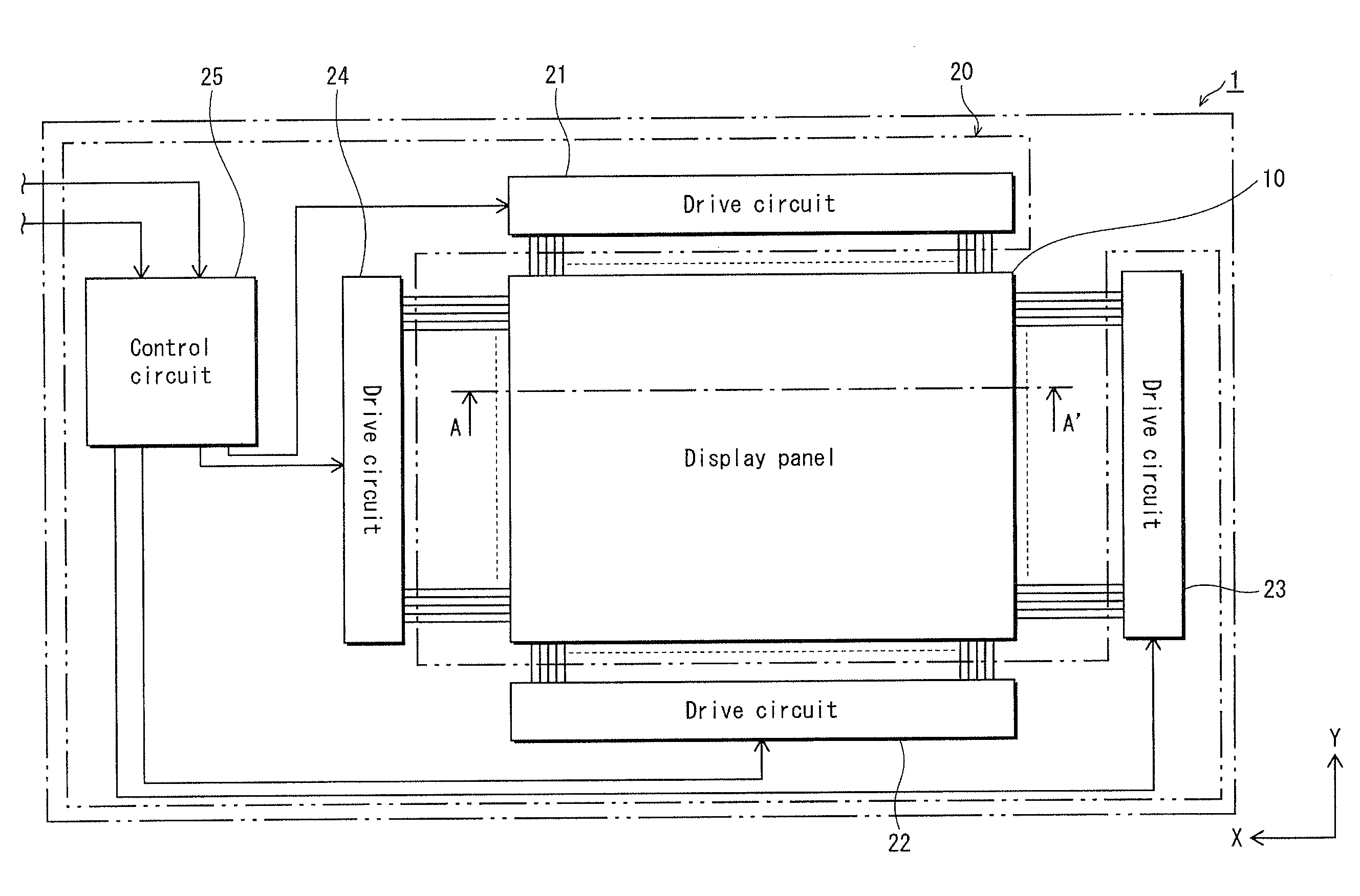
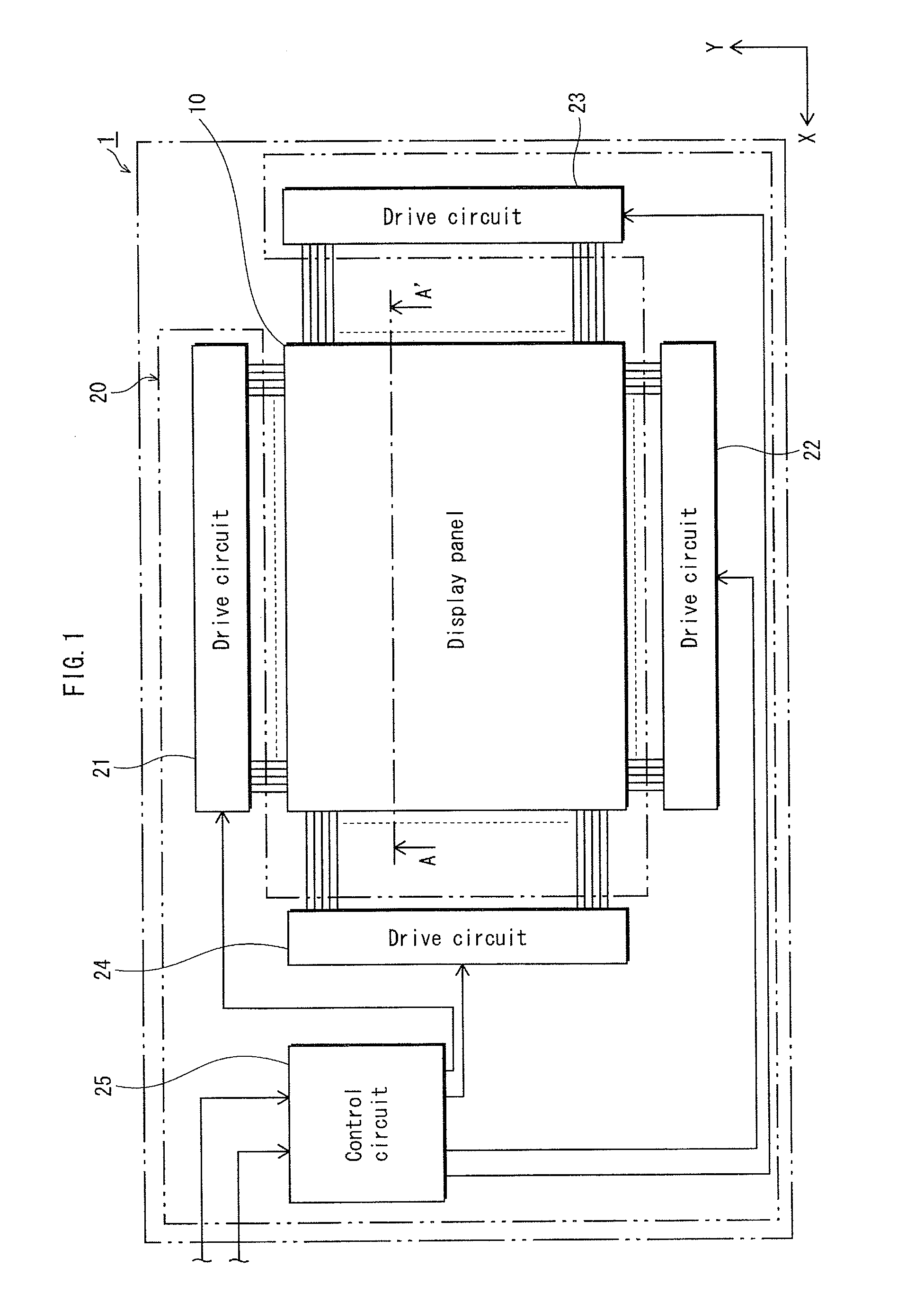
[0094]1. Configuration of Display Device 1

[0095]The overall structure of the display device 1 according to the present Embodiment is described with reference to FIG. 1.

[0096]As shown in FIG. 1, the display device (organic display device) 1 includes a display panel unit 10 and a drive control unit 20 connected to the display panel unit 10. The display panel unit 10 is an organic light-emitting panel that uses the phenomenon of electroluminescence occurring in organic material and is composed of a plurality of pixels arrayed two-dimensionally in the X-Y plane direction.

[0097]The drive control unit 20 is ...

modification 1

[Modification 1]

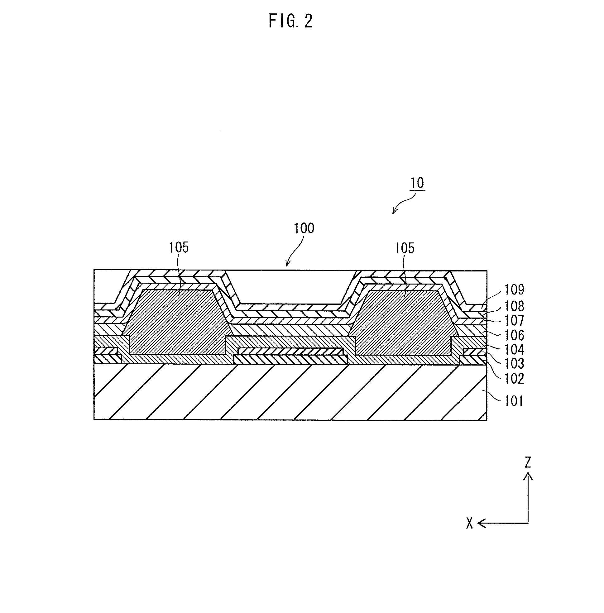
[0173]Next, with reference to FIG. 12, Modification 1 of the manufacturing method of the display device 1 is described. FIG. 12 illustrates processes corresponding to processes illustrated in FIGS. 9C to 10A.

[0174]As shown in FIG. 12, first a bank material layer 1050 is formed to cover the hole injection transporting layer 104, and then a mask 503 is placed above the bank material layer 1050. The mask 503 is provided with light transmissive portions 503a1, 503a2, 503b, 503c, 503d1, and 503d2. The light transmissive portions 503a1 and 503a2 are provided at locations corresponding to a portion in which the bank 105a is to be formed; the light transmissive portion 503b is provided at a location corresponding to a portion in which the bank 105b is to be formed; the light transmissive portion 503c is provided at a location corresponding to a portion in which the bank 105c is to be formed; and the light transmissive portions 503d1 and 503d2 are provided at locations corres...

modification 2

[Modification 2]

[0181]Next, with reference to FIGS. 13 and 14, Modification 2 of the manufacturing method of the display device 1 is described. FIGS. 13A to 14B illustrate processes corresponding to the processes illustrated in FIGS. 9C to 10B.

[0182]As shown in FIG. 13A, first a bank material layer 1050 is formed to cover the hole injection transporting layer 104, and then a mask 504 is placed above the bank material layer 1050. The mask 504 has openings 504a, 504b, 504c, and 504d corresponding to the portions at which banks 105 are to be formed.

[0183]The openings 504b and 504c are formed to have the same width as the openings 501b and 501c in the mask 501 used in the manufacturing method of the above Embodiment.

[0184]On the other hand, a width Wa3 of the opening 504a located between the planned sub-pixel formation region 1000a and the planned non-light-emitting cell formation region 1000d in correspondence with the bank 105a that is to be formed (see FIG. 4) is set to be larger tha...


PUM


Abstract

A pixel in the panel includes sub-pixels 100a, 100b, and 100c. Non-light-emitting cells 100d and 100e are provided between the pixel and adjacent pixels on both sides thereof, respectively. The organic light-emitting layer of sub-pixel 100a and non-light-emitting cell 100d are separated by bank 105a. Similarly, the organic light-emitting layer of sub-pixel 100c and non-light-emitting cell 100e are separated by bank 105d; the organic light-emitting layers of sub-pixels 100a and 100b are separated by bank 105b; and the organic light-emitting layers of sub-pixels 100b and 100c are separated by bank 105c. Inclination angle θaa of sidewall 105aa of bank 105a adjacent to sib-pixel 100a and inclination angle θdc of sidewall 105dc of bank 105d adjacent to sib-pixel 100c are larger than other inclination angles θba, θbb, θcb, and θcc.

Description

[0001]This is a continuation application of PCT Application No. PCT / JP2010 / 006149 filed on Oct. 15, 2010, designating the United States of America, the disclosure of which, including the specification, drawings and claims, is incorporated herein by reference in its entirety.TECHNICAL FIELD[0002]The present invention relates an organic light-emitting panel, a manufacturing method thereof, and an organic display device.BACKGROUND ART[0003]In recent years, progress has been made in the research and development of display devices that use the phenomenon of electroluminescence occurring in organic material. Each light-emitting cell of such a display device is composed of an anode and a cathode with an organic light-emitting layer therebetween. When the display device is driven, holes are injected through the anode, electrons are injected through the cathode, and the holes and electrons recombine within the organic light-emitting layer, thereby emitting the light.[0004]Banks composed of i...

Claims


Application Information

Patent Timeline
Patent Type & Authority Applications(United States)
IPC IPC(8): H01L51/52H01L51/56
CPCH01L27/3218H01L27/3223H05B33/10H01L51/0005H01L27/3246H10K59/88H10K59/353H10K71/135H10K59/122H10K59/123
Inventor MATSUSHIMA, HIDEAKI
Owner JOLED INC
Why Eureka
Try Eureka