Check patentability & draft patents in minutes with Patsnap Eureka AI!

Semiconductor memory device

a memory device and semiconductor technology, applied in the direction of information storage, static storage, digital storage, etc., can solve the problems of insufficient voltage level and failure of semiconductor memory devices, and achieve the effect of improving operational stability and minimizing leakage curren

Active Publication Date: 2012-08-02
SK HYNIX INC
View PDF2 Cites 12 Cited by
  • Summary
  • Abstract
  • Description
  • Claims
  • Application Information

AI Technical Summary

Benefits of technology

[0024]Exemplary embodiments of the present invention are directed to a semiconductor memory device which may minimize the leakage current and / or improve the operational stability by using a circuit that performs a pre-charge driving operation of sub-word lines through systematic timing control.

Problems solved by technology

However, there are several concerns regarding the pre-charge operation of the known semiconductor memory device adopting the negative word line driving scheme.
Thus, the voltage level may not be sustained for a sufficient time.
Therefore, the semiconductor memory device may fail.

Method used


Image

  • Semiconductor memory device
  • Semiconductor memory device
  • Semiconductor memory device

Examples


Embodiment Construction

[0032]Exemplary embodiments of the present invention will be described below in more detail with reference to the accompanying drawings. The present invention may, however, be embodied in different forms and should not be construed as limited to the embodiments set forth herein. Rather, these embodiments are provided so that this disclosure will be thorough and complete, and will fully convey the scope of the present invention to those skilled in the art. Throughout the disclosure, like reference numerals refer to like parts throughout the various figures and embodiments of the present invention.

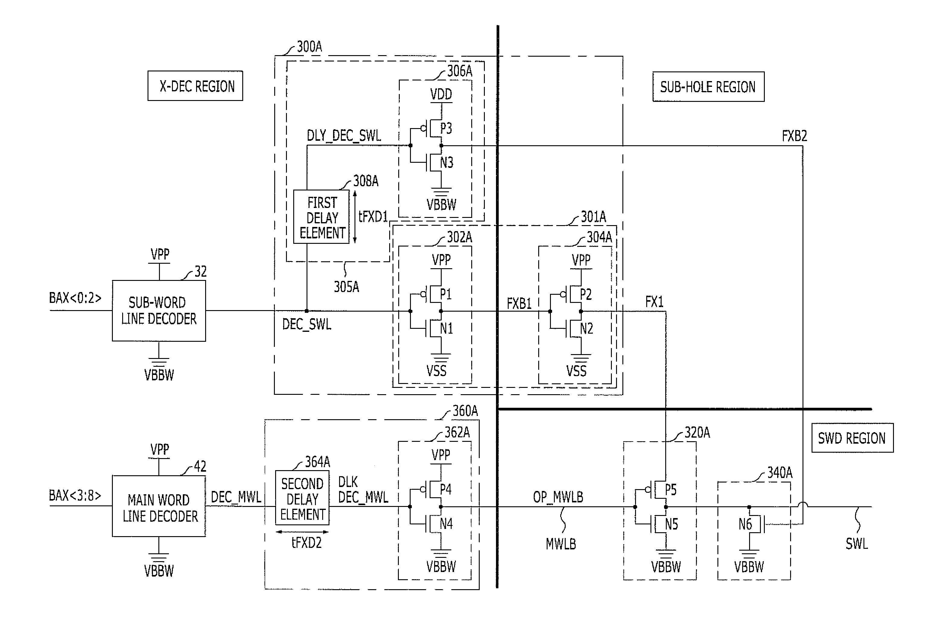
[0033]FIGS. 3A and 3B are circuit diagrams illustrating semiconductor memory devices adopting a negative word line driving scheme in accordance with exemplary embodiments of the present invention.

[0034]Referring to FIG. 3A, the semiconductor memory device adopting a negative word line driving scheme in accordance with an exemplary embodiment of the present invention includes: a main word lin...


PUM


Abstract

A semiconductor memory device includes a main word line signal generator configured to generate a main word line signal having a first swing width, a sub-word line signal generator configured to generate a first sub-word line signal and a second sub-word line signal having a second swing width and a third swing width, respectively, a first sub-word line driver configured to drive a corresponding sub-word line with the first sub-word line signal or a negative word line voltage in response to the main word line signal, and a second sub-word line driver configured to drive the corresponding sub-word line with the negative word line voltage in response to the second sub-word line signal.

Description

CROSS-REFERENCE TO RELATED APPLICATIONS[0001]The present application claims priority of Korean Patent Application No. 10-2011-0008936, filed on Jan. 28, 2011, which is incorporated herein by reference in its entirety.BACKGROUND[0002]1. Field of the Invention[0003]Exemplary embodiments of the present invention relate to a semiconductor device design, and more particularly, to a semiconductor memory device which drives negative word lines.[0004]2. Description of the Related Art[0005]A negative word line driving method is a method performed by a word line driving circuit that drives word lines by applying a high voltage VPP to a word line to enable the word line and applying a voltage VBBW lower than a ground voltage VSS to the word line to disable the word line. In general, the ground voltage VSS is applied to a word line to disable the word line, but according to the negative word line driving method, a voltage VBBW lower than a ground voltage VSS is applied to the word line to disab...

Claims


Application Information

Patent Timeline
IPC IPC(8): G11C7/00
CPCG11C8/08G11C8/18G11C5/14
Inventor LEE, DONG-GEUNDO, CHANG-HO
Owner SK HYNIX INC
Features
  • R&D
  • Intellectual Property
  • Life Sciences
  • Materials
  • Tech Scout
  • Unparalleled Data Quality
  • Higher Quality Content
  • 60% Fewer Hallucinations
Learn More