Systems and methods for dynamic mosfet body biasing for low power, fast response VLSI applications

a dynamic mosfet body and biasing technology, applied in the field of operation of metaloxidesemiconductor field-effect transistors, can solve the problems of increasing power consumption, leakage current becoming a bigger factor of the total power consumption of transistors, and the miniaturization of transistors, so as to increase the response time and minimize leakage current

Inactive Publication Date: 2012-08-16
CALIFORNIA INST OF TECH
View PDF9 Cites 8 Cited by
  • Summary
  • Abstract
  • Description
  • Claims
  • Application Information

AI Technical Summary

Benefits of technology

[0007]Systems and methods in accordance with embodiments of the invention include MOSFET transistor operation by adjusting Vbs, or the voltage applied to the body terminal of the MOSFET transistor, to control the threshold voltage (Vth) in order to minimize leakage current and increase response time. One embodiment includes a n-channel metal-oxide-semiconductor field-effect transistor (NMOS), including: a gate terminal; a source terminal; a drain terminal; a body terminal; and control circuitry, where the control circuitry is configured to bias the body terminal at a first voltage when voltage applied to the gate terminal turns the transistor OFF and a second voltage when voltage applied to the gate terminal turns the transistor ON; and where the first voltage is of a lower value than the second voltage.

Problems solved by technology

Although miniaturization, such as decreasing transistor size to 50 nm and below, holds important design benefits in allowing for greater processing power in equal or smaller space, there are also design tradeoffs, such as increased power consumption due to both dynamic and leakage current, that serves as a constraint to inhibit the advantages of transistor feature size reduction.
Additionally, the leakage current becomes a bigger factor of the total power consumption of transistors as well as transistors are miniaturized.

Method used


Image

  • Systems and methods for dynamic mosfet body biasing for low power, fast response VLSI applications
  • Systems and methods for dynamic mosfet body biasing for low power, fast response VLSI applications
  • Systems and methods for dynamic mosfet body biasing for low power, fast response VLSI applications

Examples


Embodiment Construction

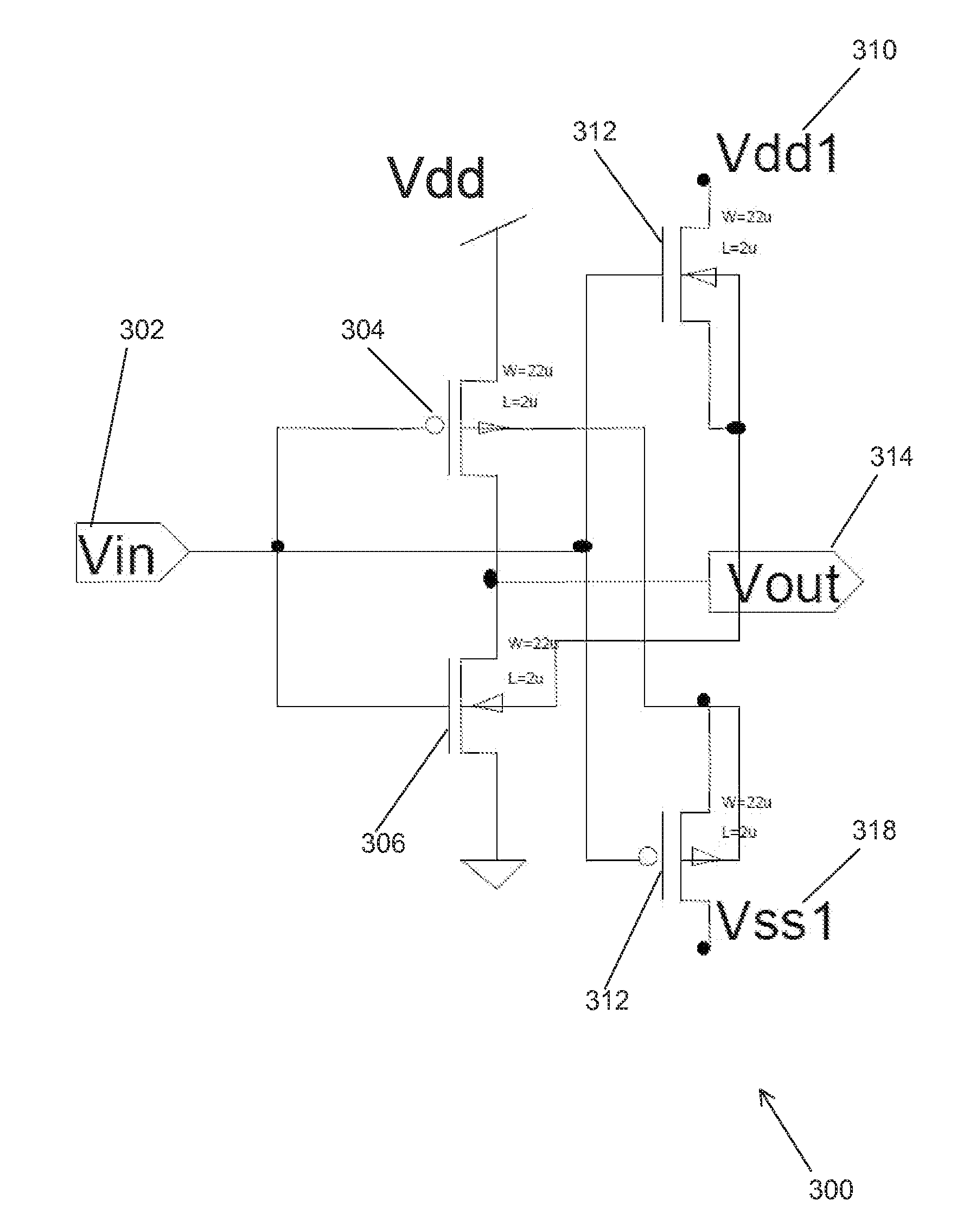
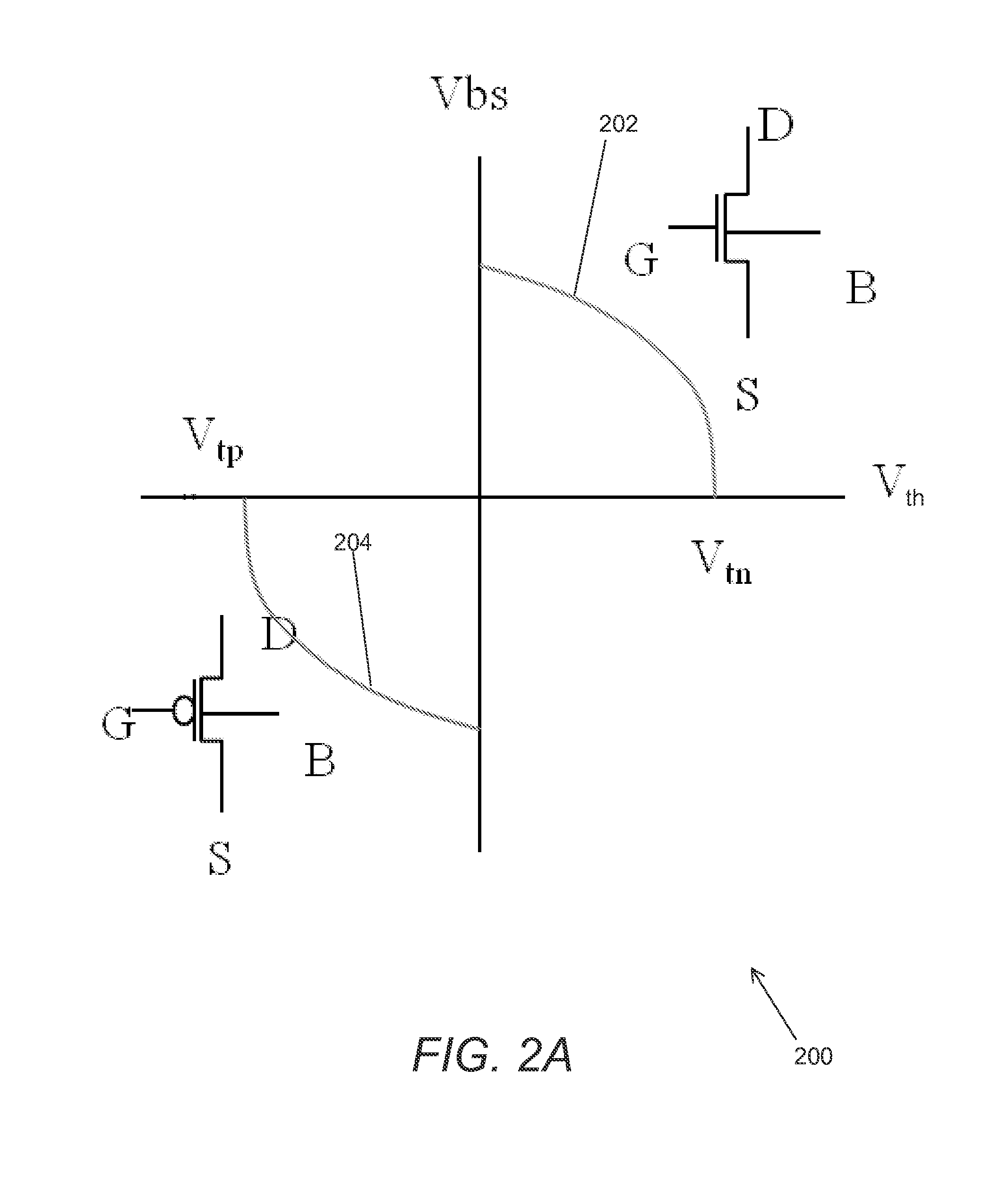
[0037]Turning now to the drawings, systems and methods for MOSFET transistor operation involving adjusting Vbs, or the voltage applied to the body terminal of the MOSFET transistor, to control the threshold voltage (Vth) in order to minimize leakage current and increase response time in accordance with embodiments of the invention are illustrated. In many embodiments, Vbs is controlled to have a low absolute value so that Vth is high when a transistor is non-active, or OFF. Likewise in numerous embodiments, Vbs is controlled to have a high absolute value so that Vth is low when a transistor is active, or ON.

[0038]Furthermore, dynamically biasing a transistor's body dependent upon its intended operational state allows for a reduction of leakage current and wasted power during a transistor's off state by raising Vth. Additionally, dynamically biasing a transistor's body also allows for a faster and more effective response time for a transistor's ON state by reducing Vth when a transis...


PUM


Abstract

Systems and methods in accordance with embodiments of the invention are disclosed that include MOSFET transistor operation by adjusting Vbs, or the voltage applied to the body terminal of the MOSFET transistor, to control the threshold voltage (Vth) in order to minimize leakage current and increase response time. One embodiment includes a n-channel metal-oxide-semiconductor field-effect transistor (NMOS), including: a gate terminal; a source terminal; a drain terminal; a body terminal; and control circuitry, where the control circuitry is configured to bias the body terminal at a first voltage when voltage applied to the gate terminal turns the transistor OFF and a second voltage when voltage applied to the gate terminal turns the transistor ON; and where the first voltage is of a lower value than the second voltage.

Description

CROSS-REFERENCE TO RELATED APPLICATIONS[0001]The current application claims priority to U.S. Provisional Application No. 61 / 442,371, filed Feb. 14, 2011, the disclosure of which is incorporated herein by reference.STATEMENT OF FEDERALLY SPONSORED RESEARCH[0002]The invention described herein was made in the performance of work under a NASA contract, and is subject to the provisions of Public Law 96-517 (35 USC 202) in which the Contractor has elected to retain title.FIELD OF THE INVENTION[0003]The present invention generally relates to transistor operation and more specifically to the operation of metal-oxide-semiconductor field-effect transistors (MOSFET).BACKGROUND OF THE INVENTION[0004]Electronic systems can be built of transistors to amplify or switch electronic signals. A transistor is typically composed of a semiconductor material with at least three terminals for connection to an external circuit. In a transistor, typically a voltage or current applied to one pair of the trans...

Claims


Application Information

Patent Timeline
Patent Type & Authority Applications(United States)
IPC IPC(8): H03K17/687
CPCH03K2217/0018H03K17/302
Inventor DUONG, TUAN ANH
Owner CALIFORNIA INST OF TECH
Why Eureka
Try Eureka