Method for fabricating CMOS image sensor

Inactive Publication Date: 2006-01-05
DONGBU ELECTRONICS CO LTD
View PDF21 Cites 7 Cited by
  • Summary
  • Abstract
  • Description
  • Claims
  • Application Information

AI Technical Summary

Benefits of technology

[0031] An object of the present invention is to provide a method for fabricatin

Problems solved by technology

The CCD has the high power consumption and the complicated mask process.
Also, it is impossible to provide the signal processing circ

Method used


Image

  • Method for fabricating CMOS image sensor
  • Method for fabricating CMOS image sensor
  • Method for fabricating CMOS image sensor

Examples


Embodiment Construction

[0039] Reference will now be made in detail to the preferred embodiments of the present invention, examples of which are illustrated in the accompanying drawings. Wherever possible, the same reference numbers will be used throughout the drawings to refer to the same or like parts.

[0040] Hereinafter, a method for fabricating a CMOS image sensor according to the present invention will be described with reference to the accompanying drawings.

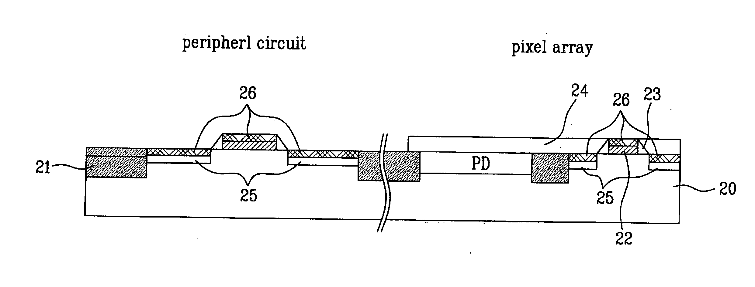
[0041] Generally, in a pixel array, a gate electrode requires a low resistance. Accordingly, preferably, a salicide layer is formed in the pixel array. However, the salicide layer may not be formed in source and drain junctions.

[0042] In a readout circuit of a pixel array according to the present invention, a salicide layer is formed on a gate electrode, and is not formed in source and drain junctions.

[0043]FIG. 3A to FIG. 3F are cross sectional views of the process for fabricating a CMOS image sensor according to the present invention, wherein...


PUM


Abstract

A method for fabricating a CMOS image sensor is disclosed, to minimize the leakage current and to improve the yield, which includes the steps of preparing a semiconductor substrate including a peripheral circuit and a pixel array, wherein the pixel array is comprised of a photodiode and a readout circuit; defining an active area and a field area in the semiconductor substrate; forming a field oxide layer in the field area of the semiconductor substrate; forming gate electrodes in the peripheral circuit and the readout circuit of the pixel array; forming a photodiode in a photodiode portion of the pixel array; forming source and drain junctions at both sides of the gate electrode in the semiconductor substrate of the active area; forming a salicide prevention layer in the semiconductor substrate of the pixel array; and forming salicide layers in the surface of the gate electrode and the source and drain junctions in the peripheral circuit by using the salicide prevention layer as a mask.

Description

CROSS-REFERENCE TO RELATED APPLICATIONS [0001] This application claims the benefit of Korean Application No. P2004-52007 filed on Jul. 5, 2004, which is hereby incorporated by reference as if fully set forth herein. BACKGROUND OF THE INVENTION [0002] 1. Field of the Invention [0003] The present invention relates to a method for fabricating an image sensor, and more particularly, to a method for fabricating a CMOS image sensor to decrease a leakage current. [0004] 2. Discussion of the Related Art [0005] Generally, an image sensor is a semiconductor device for converting an optical image into an electric signal. The image sensor can be broadly categorized into a charge coupled device (CCD) and a complementary metal oxide semiconductor (CMOS) image sensor. [0006] In case of the CCD, respective metal-oxide-silicon MOS capacitors are positioned adjacently, wherein electric charge carriers are stored in and transferred to the capacitors. Meanwhile, the CMOS image sensor adopts the CMOS te...

Claims


Application Information

Patent Timeline
IPC IPC(8): H01L31/062H01L21/8234H01L27/088H01L27/146H04N5/335H04N5/361H04N5/369H04N5/374
CPCH01L27/1462H01L27/14689H01L27/1463H01L27/146H01L31/10
Inventor JEON, IN GYUN
Owner DONGBU ELECTRONICS CO LTD
Why Eureka
Try Eureka