Solar cell and method for manufacturing such a solar cell

a solar cell and manufacturing method technology, applied in the field of solar cells, can solve the problems of reducing the yield of the manufacturing process, adversely affecting the efficiency of the solar cell, and contaminating the front side of the substrate,

Active Publication Date: 2012-08-16
NEDERLANDSE ORG VOOR TOEGEPAST NATUURWETENSCHAPPELIJK ONDERZOEK TNO
View PDF6 Cites 6 Cited by
  • Summary
  • Abstract
  • Description
  • Claims
  • Application Information

AI Technical Summary

Benefits of technology

[0007]It is an object of the present invention to provide a method for manufacturing the solar cell with p- or n-type base, which overcomes or reduces the disadvantages as mentioned above.
[0009]Advantageously, the method provides an enhanced manufacturing with less variation between individual solar cells: A parasitic doping (either p-type or n-type) from one surface of the silicon substrate to another surface, especially from the BSF side to the emitter side, is prevented in an easy way by the method. Also, a screen printing step is omitted which reduces yield loss due to breakage. Moreover, two-sided diffusion of phosphorus in both front and back surfaces allows an improved gettering of impurities from the silicon substrate.
[0040]Also advantageously, the method may result in higher efficiency of the solar cells due to improved surface passivation of surfaces with doped layers, when the texture features on these surfaces are (even slightly) smoothened.Also, the invention relates to a solar cell comprising a semiconductor substrate of a first conductivity type having a textured front surface and a back surface, wherein the textured front surface comprises a second conductivity-type doped layer, wherein the back surface comprises a surface field layer of the first conductivity type.In an embodiment, the invention relates to the solar cell as described above, wherein the textured front surface comprises a pyramidal shapes containing front surface with intermediate valleys having widths selected from the range of 50-500 nm.In an embodiment, the invention relates to the solar cell as described above, wherein the textured front surface has valleys with curvatures having radii selected from the range of 25-250 nm.

Problems solved by technology

The screen printing method to form the BSF layer on the back side may cause contamination of the front side of the substrate by parasitic diffusion or spill over of the dopant source to the front side.
Parasitic diffusion of the dopant on the front side results in a non-uniform dopant concentration profile for the emitter layer which will adversely affect the efficiency of the solar cell.
Furthermore, screen printing reduces the yield of the manufacturing process due to a relatively high chance of breakage of substrates.
Also, for n-type BSF layers that use phosphorus as n-type dopant, a one-sided diffusion results in a less efficient gettering of impurities from the substrate.

Method used


Image

  • Solar cell and method for manufacturing such a solar cell
  • Solar cell and method for manufacturing such a solar cell
  • Solar cell and method for manufacturing such a solar cell

Examples


Embodiment Construction

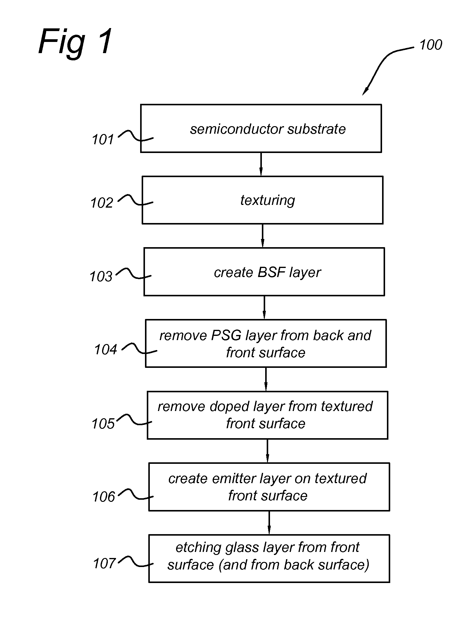
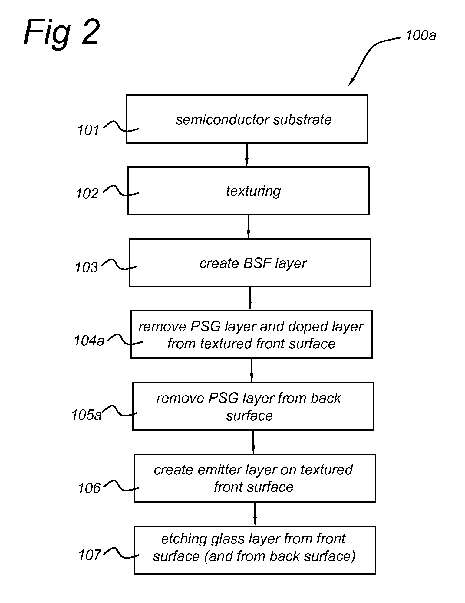
[0062]FIG. 1 shows a flow diagram for a method for manufacturing a solar cell in accordance with a first aspect of the invention.

[0063]According to the first aspect, the method comprises a sequence 100 of processes to manufacture a solar cell with either p- or n-type base.

[0064]Below, the sequence 100 is illustrated for a solar cell with n-type base.

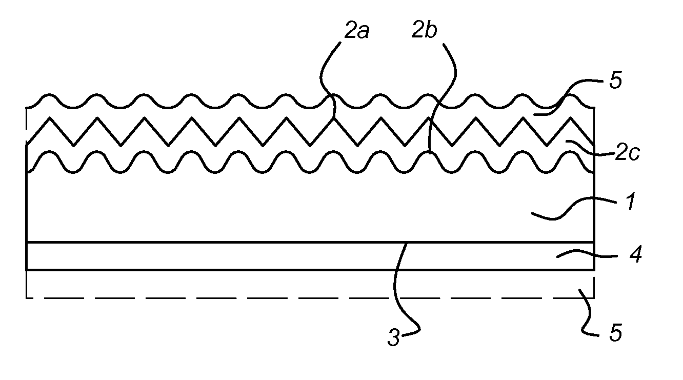
[0065]A single crystal or multi-crystalline semiconductor substrate i.e., a silicon substrate 1 with n-type conductivity is provided as precursor for the solar cell. The silicon substrate has a front surface 2 and a back surface 3. The front surface is arranged as surface for receiving light during use of the solar cell.

[0066]In an alternative embodiment, the silicon substrate is doped to have a conductivity of p-type.

[0067]FIG. 5 shows a cross-section of the silicon substrate for manufacturing the solar cell.

[0068]Referring again to FIG. 1, next, in process 102, the method provides texturing of the surfaces 2, 3 of the silicon substrate...


PUM


Abstract

A method (100; 100a; 100b; 100c) for manufacturing a solar cell from a semiconductor substrate (1) of a first conductivity type, the semiconductor substrate having a front surface (2) and a back surface (3). The method includes in a sequence: texturing (102) the front surface to create a textured front surface (2a); creating (103) by diffusion of a dopant of the first conductivity type a first conductivity-type doped layer (2c) in the textured front surface and a back surface field layer (4) of the first conductivity type in the back surface; removing (105; 104a) the first conductivity-type doped layer from the textured front surface by an etching process adapted for retaining texture of the textured front surface; creating (106) a layer of a second conductivity type (6) on the textured front surface by diffusion of a dopant of the second conductivity type into the textured front surface.

Description

FIELD[0001]The present invention relates to a solar cell. Also, the present invention relates to a method for manufacturing such a solar cell.BACKGROUND[0002]Such a solar cell relates to a solar cell with p- or n-type base.[0003]The solar cell comprises a semiconductor substrate, e.g. silicon, which is covered on a back side by the p- or n-type back surface field (BSF) layer and on a front side by an emitter layer of a conductivity type opposite to that of the base layer. The front side of the substrate is arranged to be directed towards a light source during use of the solar cell.[0004]In the prior art, the p- or n-type back surface field layer (BSF layer), is for example manufactured by a screen printing process (but also POCl3 face-to-face tube furnace diffusion, spray coating, spin coating, etc. can be used). During the screen printing process, a paste that comprises a p- or n-type element as dopant element is printed one-sidedly on the back side of the substrate. Next, a first ...

Claims


Application Information

Patent Timeline
Patent Type & Authority Applications(United States)
IPC IPC(8): H01L31/0236H01L31/18
CPCH01L31/18H01L31/02363Y02E10/50Y02E10/547Y02E10/548H01L31/068H01L31/02167
Inventor BARTON, PAUL CORNELISNABER, RONALD CORNELIS GERARDSTASSEN, ARNO FERDINAND
Owner NEDERLANDSE ORG VOOR TOEGEPAST NATUURWETENSCHAPPELIJK ONDERZOEK TNO
Why Eureka
Try Eureka