Silicon germanium film formation method and structure
- Summary
- Abstract
- Description
- Claims
- Application Information
AI Technical Summary
Benefits of technology
Problems solved by technology
Method used
Image

Examples
Embodiment Construction
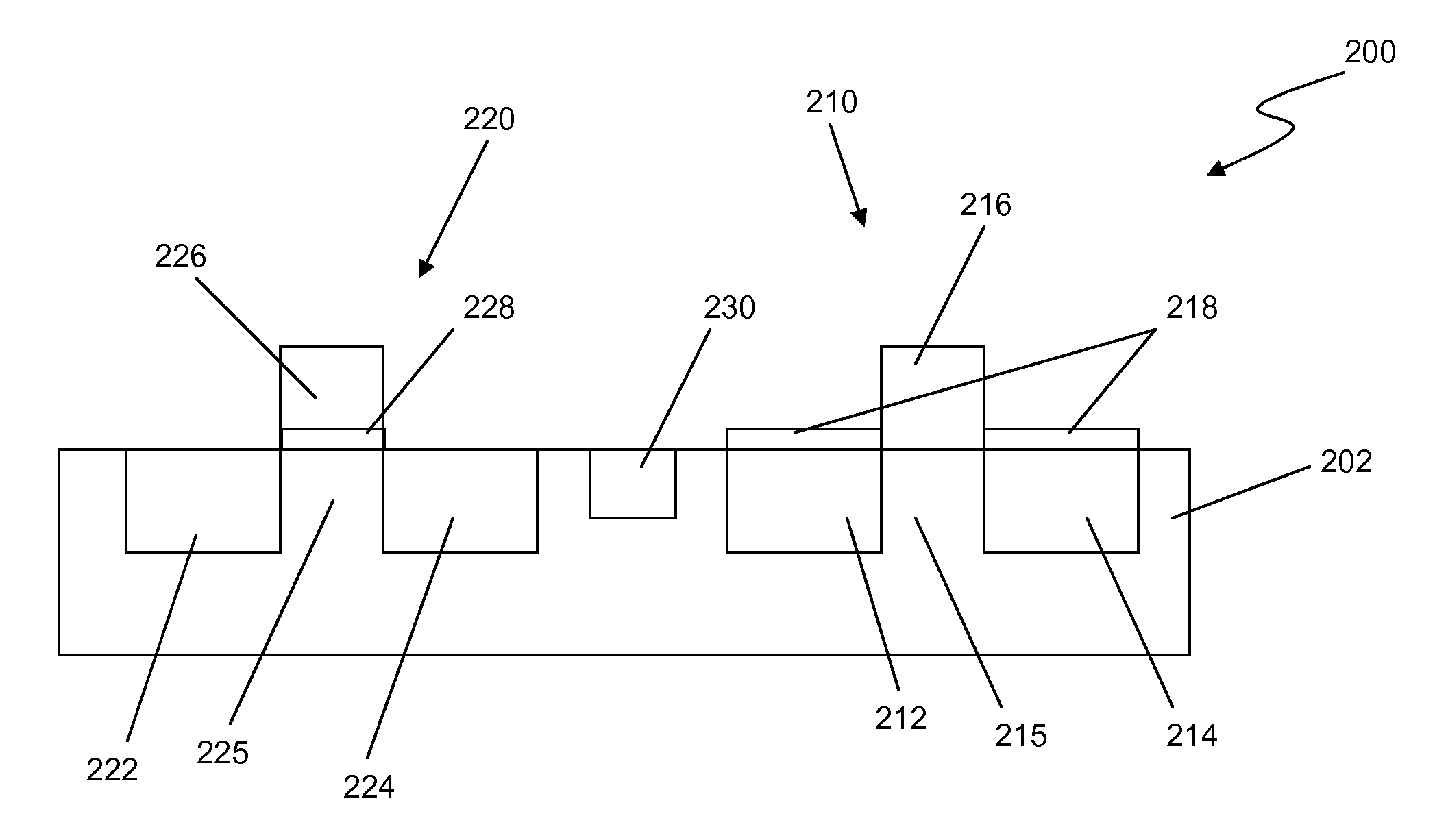
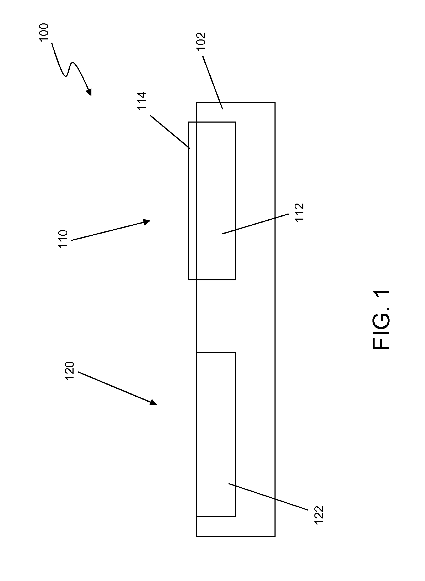
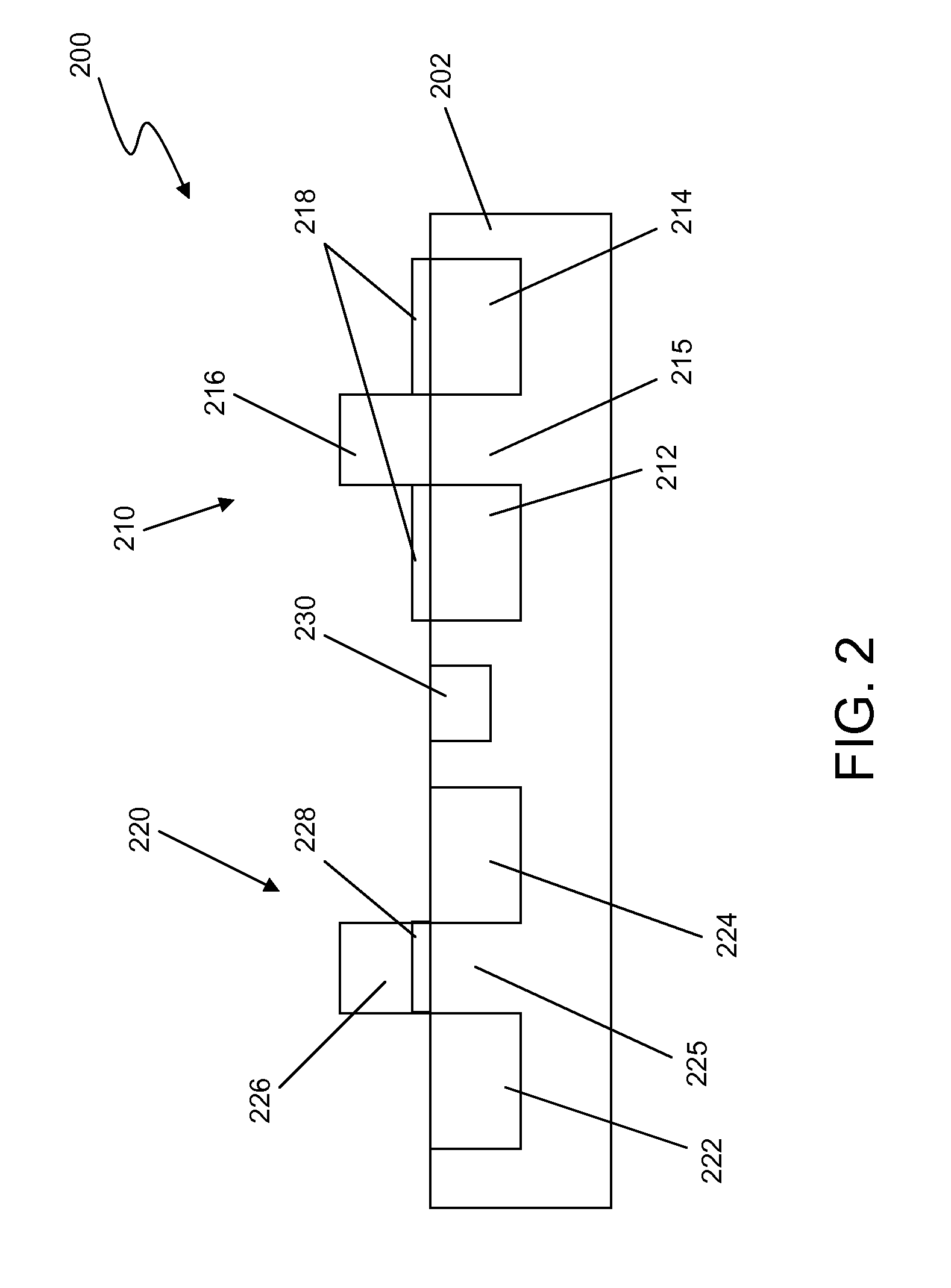
[0016]With reference now to FIG. 1, a semiconductor device 100 is shown and in embodiments is made with a manufacturing method starting with providing a substrate 102. A first region 110 of substrate 102 may be doped with a first dopant 112 in a first concentration, and a second region 120 of substrate 102 may be doped with a second dopant 122 in a second concentration. In an embodiment, second region 120 is left undoped or is considered to have a zero concentration of second dopant 122. Doping may be performed using ion implantation or any other suitable technique now known or later discovered within the scope of the invention.
[0017]The first and second regions 110, 120 are exposed to another material, such as silicon germanium (SiGe), for a predetermined period of time to form a layer 114 of the material over desired portions of substrate 102, such as first region 110 doped with first dopant 112. The exposure to the material may be achieved by exposing substrate 102 to a stream of...
PUM
 Abstract
Description
Claims
Application Information
 - R&D
- Intellectual Property
- Life Sciences
- Materials
- Tech Scout
- Unparalleled Data Quality
- Higher Quality Content
- 60% Fewer Hallucinations
Browse by: Latest US Patents, China's latest patents, Technical Efficacy Thesaurus, Application Domain, Technology Topic, Popular Technical Reports.
© 2025 PatSnap. All rights reserved.Legal|Privacy policy|Modern Slavery Act Transparency Statement|Sitemap|About US| Contact US: help@patsnap.com