Supercharge Your Innovation With Domain-Expert AI Agents!

METHODS OF INTEGRATING REVERSE eSiGe ON NFET AND SiGe CHANNEL ON PFET, AND RELATED STRUCTURE

a reverse esige and pfet technology, applied in the field of integrated circuit (ic) chip fabrication, can solve the problems of poor throughput, defects if not adequately removed, and added expens

Inactive Publication Date: 2009-12-03
IBM CORP +1
View PDF10 Cites 28 Cited by
  • Summary
  • Abstract
  • Description
  • Claims
  • Application Information

AI Technical Summary

Benefits of technology

[0009]A third aspect of the disclosure provides a structure comprising: an NFET having an embedded silicon germanium (SiGe) plug in a channel thereof; a PFET having a SiGe channel; and a trench isolation between the NFET and the PFET, wherein the NFET and the PFET are devoid of SiGe epitaxial growth edge effects.

Problems solved by technology

One challenge relative to fabricating these devices is preventing shifts in Vt during processing that occurs after initial formation.
Another challenge is to form both NFETs and PFETs together where each requires a different, or different concentration of, a band-edge metal.
The multiple epitaxial processes present a number of disadvantages such as added expense and poor throughput.
In addition, each selective epitaxial growth process required presents a challenge regarding removal of any residual oxide that may form on the epitaxially grown area during exposure to the environment.
More specifically, each epitaxially grown area may require an aqueous hydro-fluoric acid (HF) pre-clean and an in-situ hydrogen (H2) pre-bake prior to subsequent processing to remove any residual oxide, which may cause defects if not adequately removed.
Since the temperature of the in-situ H2 pre-bake must be controlled to prevent damage to any previously formed sections, adequate oxide removal is challenging and oftentimes results in non-uniformity issues.
Further non-uniformity and complexity issues are presented by the selective epitaxial growth processes in that the morphology of the sections being formed, and the edge effects of the sections, is defined by the openings into which the epitaxy is performed.

Method used


Image

  • METHODS OF INTEGRATING REVERSE eSiGe ON NFET AND SiGe CHANNEL ON PFET, AND RELATED STRUCTURE
  • METHODS OF INTEGRATING REVERSE eSiGe ON NFET AND SiGe CHANNEL ON PFET, AND RELATED STRUCTURE
  • METHODS OF INTEGRATING REVERSE eSiGe ON NFET AND SiGe CHANNEL ON PFET, AND RELATED STRUCTURE

Examples


Embodiment Construction

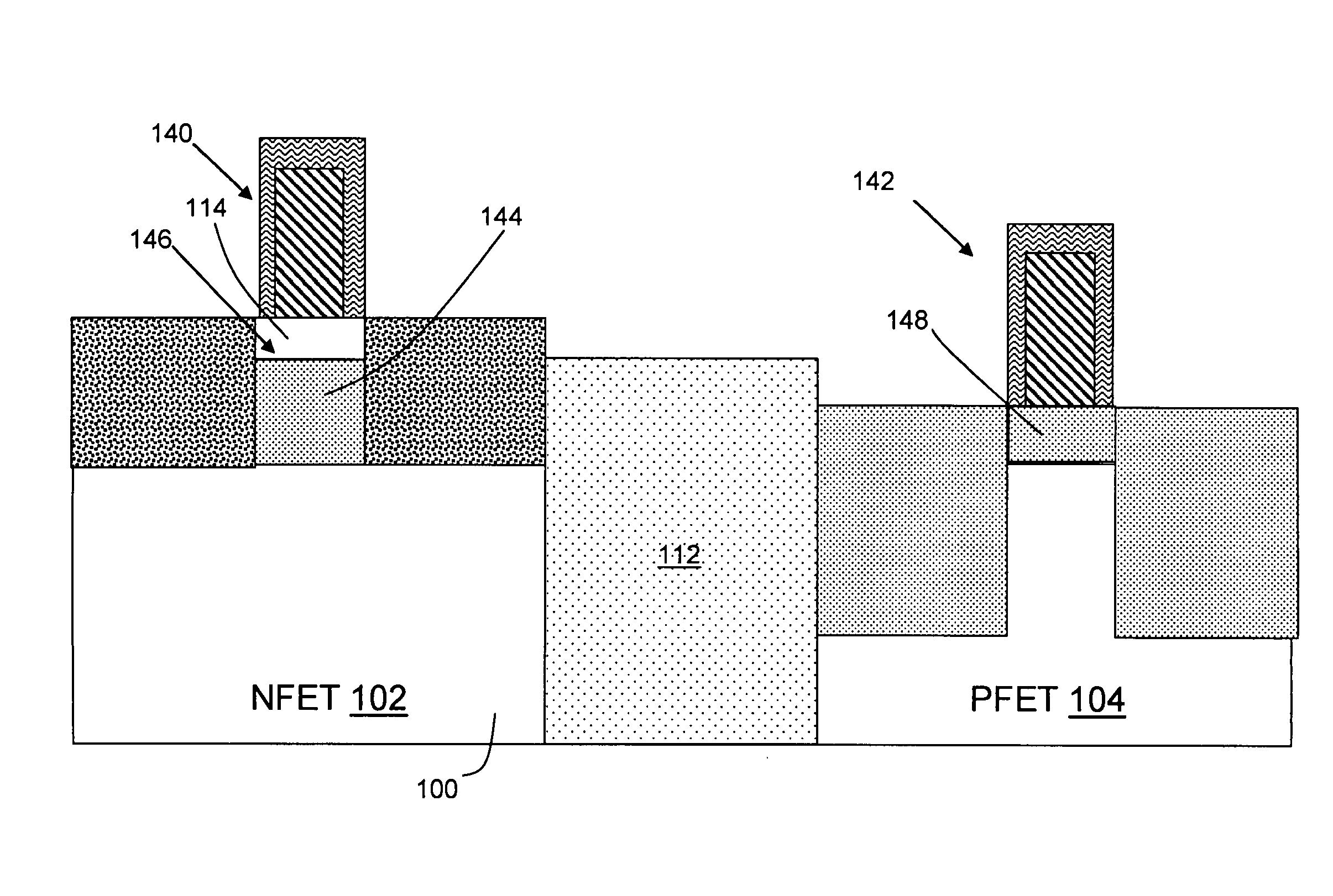
[0018]The disclosure relates to methods of forming, and related structure, a single epitaxial growth of a silicon germanium (SiGe) layer on both an n-type field effect transistor (NFET) area and p-type FET (PFET) area, which allows for process simplification. The thickness and composition of the SiGe layer in the PFET area can be separately controlled in an optional thinning process.

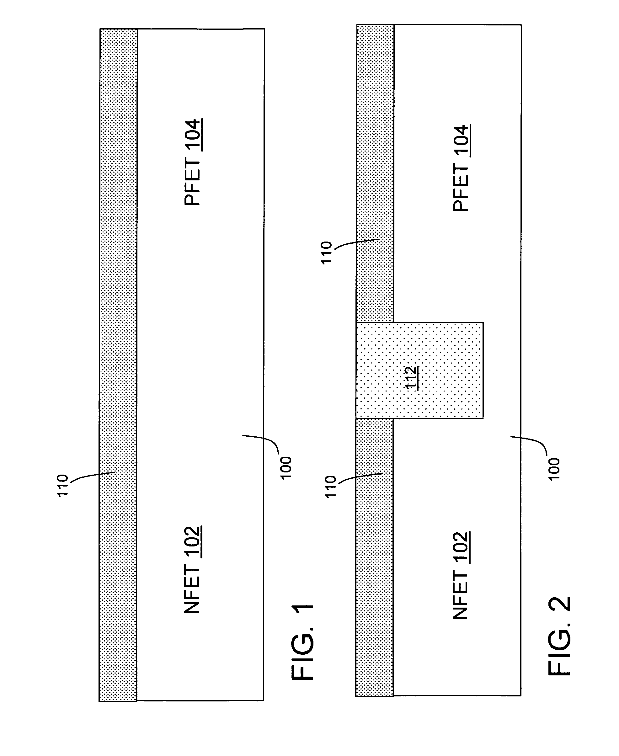
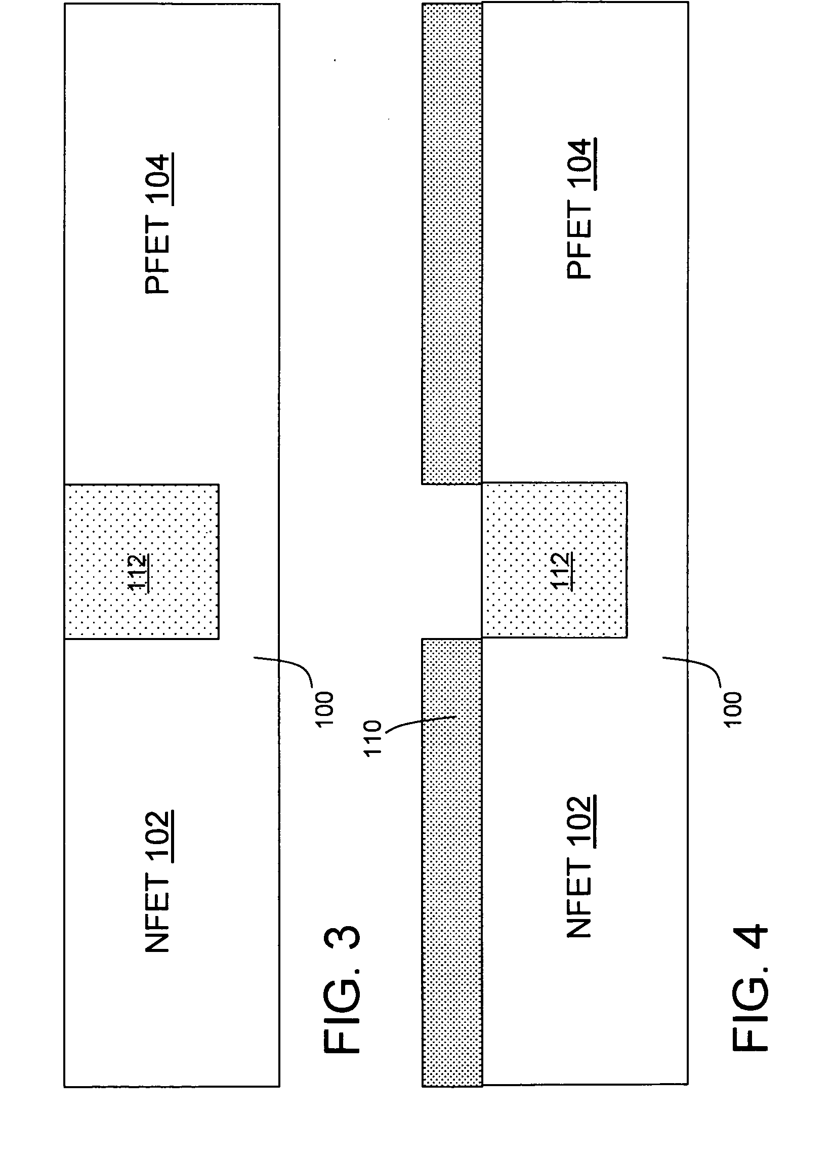
[0019]Referring to the drawings, FIG. 1 shows a first process including providing a substrate 100 including an NFET area 102 and a PFET area 102. NFET area 102 and PFET area 104 indicate regions of substrate 100 that will eventually have NFETs and PFETs formed thereon. As understood, the position of areas 102, 104 may be switched. Substrate 100 may include but is not limited to silicon, germanium, silicon germanium, silicon carbide, and those consisting essentially of one or more III-V compound semiconductors having a composition defined by the formula AlX1GaX2InX3AsY1PY2NY3SbY4, where X1, X2, X3, Y1, Y2...


PUM


Abstract

Methods of integrating reverse embedded silicon germanium (SiGe) on an NFET and SiGe channel on a PFET, and a related structure are disclosed. One method may include providing a substrate including an NFET area and a PFET area; performing a single epitaxial growth of a silicon germanium (SiGe) layer over the substrate; forming an NFET in the NFET area, the NFET including a SiGe plug in a channel thereof formed from the SiGe layer; and forming a PFET in the PFET area, the PFET including a SiGe channel formed from the SiGe layer. As an option, the SiGe layer over the PFET area may be thinned.

Description

BACKGROUND[0001]1. Technical Field[0002]The disclosure relates generally to integrated circuit (IC) chip fabrication, and more particularly, to a high-k / metal gate transistor fabrication.[0003]2. Background Art[0004]To enable high performance complementary metal-oxide semiconductor (CMOS) technologies such as high dielectric constant (high-k) and metal gate solutions, a band-edge metal is required in the channel for each transistor to maximize performance and provide threshold voltages (Vt) appropriate for low voltage, low power technologies. Different band-edge metals in the channels have been shown to work for n-type field effect transistors (NFETs) and p-type FETs (PFETs). One challenge relative to fabricating these devices is preventing shifts in Vt during processing that occurs after initial formation.[0005]Another challenge is to form both NFETs and PFETs together where each requires a different, or different concentration of, a band-edge metal. Typically, different, non-compa...

Claims


Application Information

Patent Timeline
Patent Type & Authority Applications(United States)
IPC IPC(8): H01L27/092H01L21/205H01L21/8238
CPCH01L21/823807H01L21/823814H01L29/7848H01L29/161H01L29/66636H01L29/1054
Inventor HARLEY, ERIC C. T.HOLT, JUDSON R.SCHEPIS, DOMINIC J.STEIGERWALT, MICHAEL D.BLACK, LINDACARTER, RICK
Owner IBM CORP
Features
  • R&D
  • Intellectual Property
  • Life Sciences
  • Materials
  • Tech Scout
  • Unparalleled Data Quality
  • Higher Quality Content
  • 60% Fewer Hallucinations
Learn More