LED module, method for manufacturing the same, and LED channel letter including the same

a technology of led modules and led channels, which is applied in the direction of identification means, instruments, lighting and heating apparatus, etc., can solve the problems of unfavorable bi-directional connectors facing each other, letter requires a complicated shape,

Active Publication Date: 2012-09-13
SEOUL SEMICONDUCTOR
View PDF1 Cites 8 Cited by
  • Summary
  • Abstract
  • Description
  • Claims
  • Application Information

AI Technical Summary

Benefits of technology

[0016]Another object of the present invention is to provide an LED channel letter in which an improved heat radiation route is provided between an LED in an LED module and a channel having the LED module installed therein and a route though which humidity, or the like, penetrates from the outside toward the LED in the LED module or a circuit board is reduced or block.

Problems solved by technology

This scheme requires a manual operation to cause a process defect.
In addition, when a problem occurs in only one LED module among several LED modules installed in a channel, the entire product should be replaced.
In addition, the LED channel letter requires a complicated shape in implementing a letter, a logo, a symbol, a number, and / or a sign.
However, an LED module only including only a uni-direction connector or bi-directional connectors facing each other may not easily satisfy the above-mentioned requirement.

Method used


Image

  • LED module, method for manufacturing the same, and LED channel letter including the same
  • LED module, method for manufacturing the same, and LED channel letter including the same
  • LED module, method for manufacturing the same, and LED channel letter including the same

Examples


Embodiment Construction

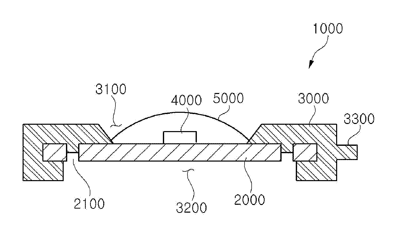
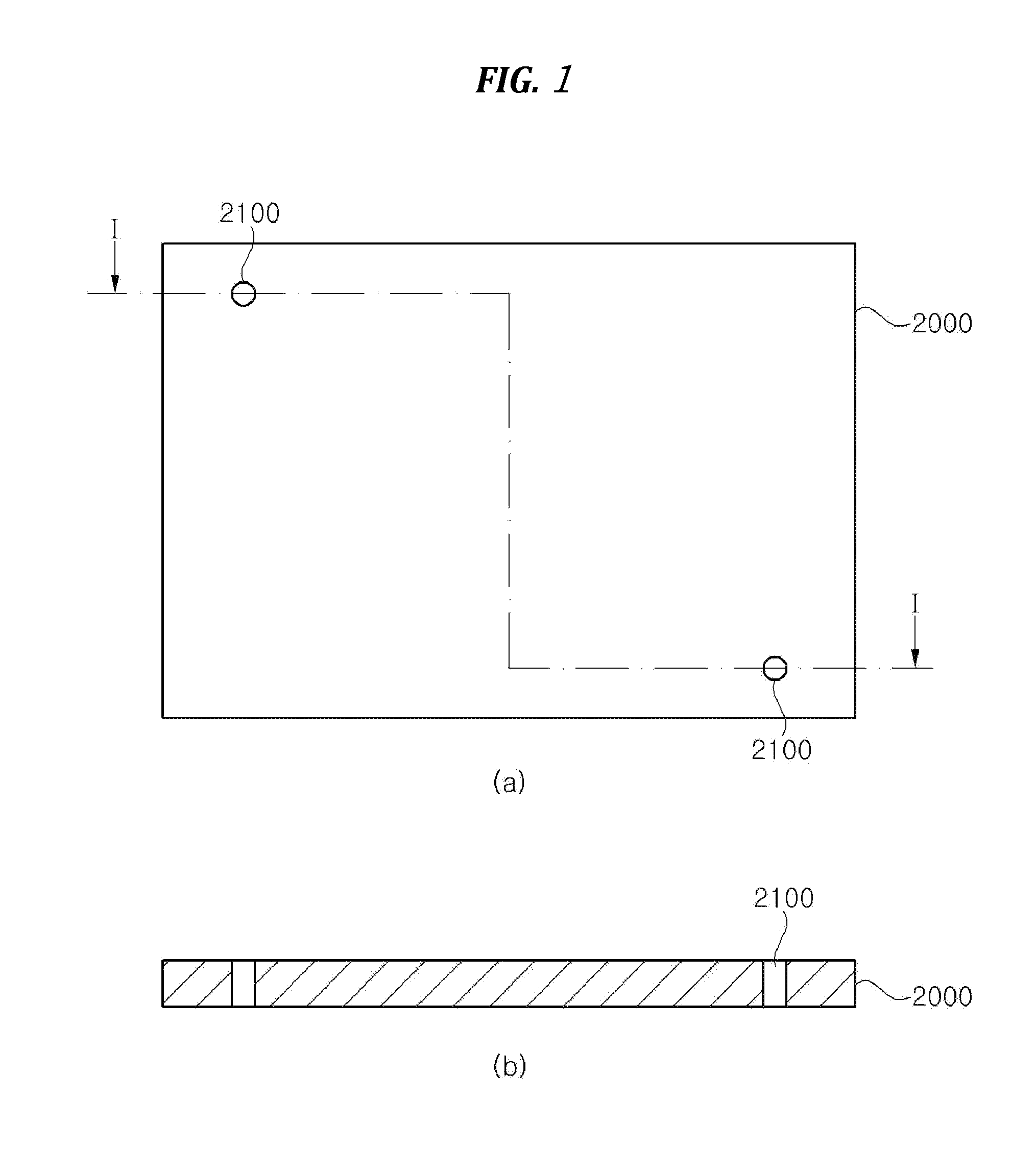
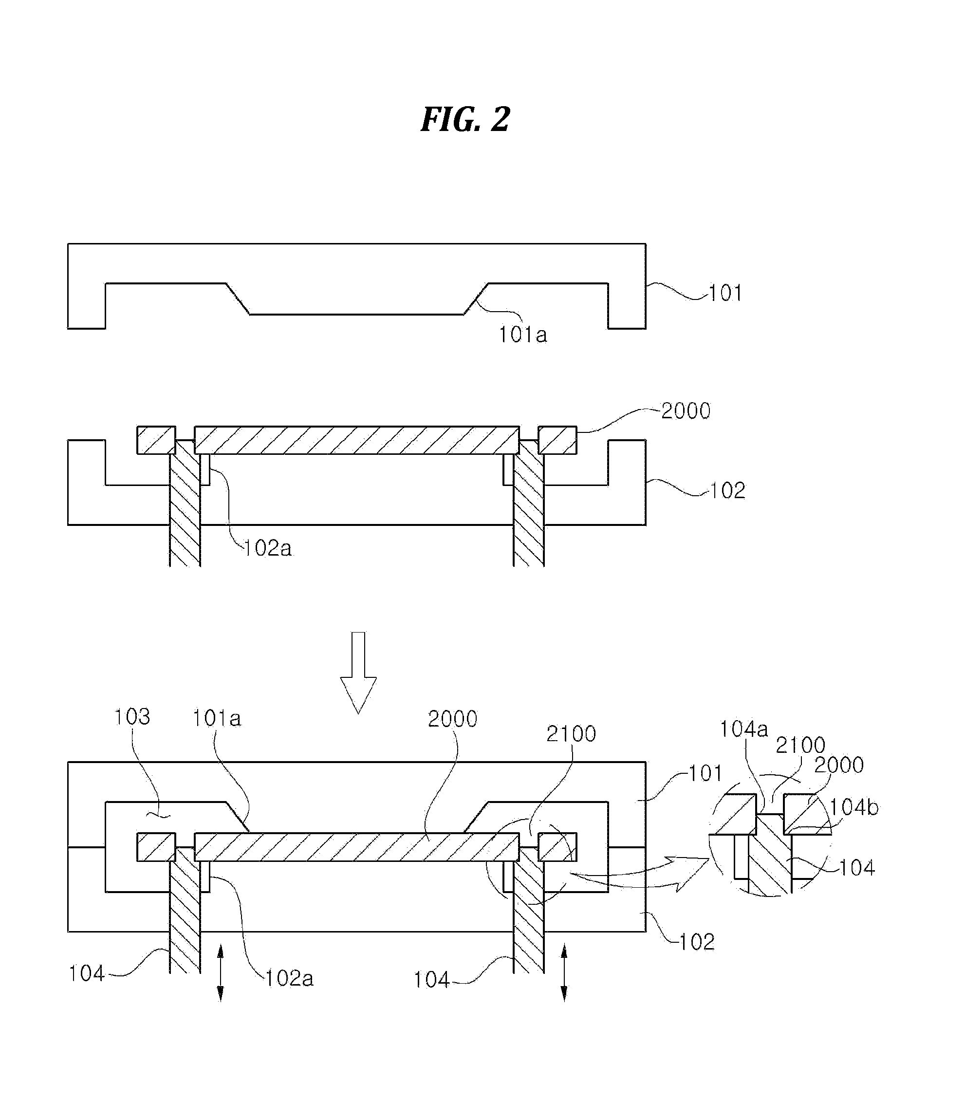
[0034]Hereinafter, exemplary embodiments of the present invention will be described in detail with reference to the accompanying drawings. The exemplary embodiments of the present invention to be described below are provided by way of example so that the idea of the present s invention can be sufficiently transferred to those skilled in the art to which the present invention pertains. Therefore, the present invention is not limited to the exemplary embodiments set forth herein but may be modified in many different forms.

[0035]In the drawings, the thickness of layers, films, panels, regions, etc., may be exaggerated for clarity. It will be understood that when an element or layer is referred to as being “on” or “connected to” another element or layer, it can be directly on or directly connected to the other element or layer, or intervening elements or layers may be present. In contrast, when an element is referred to as being “directly on” or “directly connected to” another element o...


PUM


Abstract

Disclosed herein is a method for manufacturing a light emitting diode (LED) module, the method including: disposing a circuit board at a molding space formed by an upper mold and a lower mold; adding a filling material to the molding space; hardening the filling material to form a molding cover covering at least a portion of an upper surface, a lower surface, and a side surface of the circuit board, the molding cover having an opening exposing the lower surface of the circuit board; removing the upper mold and the lower mold from the circuit board; and disposing an LED on the upper surface of the circuit board.

Description

CROSS-REFERENCE TO RELATED APPLICATIONS[0001]This application claims priority from and the benefit of Korean Patent Application No. 10-2011-0022034, filed on Mar. 11, 2011 and Korean Patent Application No. 10-2011-0022035, filed on Mar. 11, 2011, which are incorporated herein by reference for all purposes as if fully set forth herein.BACKGROUND OF THE INVENTION[0002]1. Field of the Invention[0003]Exemplary embodiments of the present invention relate to a light emitting diode (LED) module, a method for manufacturing the same, and an LED channel letter including the same.[0004]2. Discussion of the Background[0005]A cold cathode fluorescent lamp (CCFL), which is called a ‘fluorescent lamp,’ has been widely used as an illumination device for a long period of time. However, the cold cathode fluorescent lamp has disadvantages such as a short lifespan, poor durability, a limited range of color selection, and low energy efficiency.[0006]A light emitting diode (LED) has several advantages su...

Claims


Application Information

Patent Timeline
Patent Type & Authority Applications(United States)
IPC IPC(8): H01L33/58H01L33/08H01L33/52H01L33/48
CPCH01L33/486H01L33/62F21K9/00F21K9/90G09F9/33H01L2924/0002F21Y2101/02H01L2924/00F21Y2115/10
Inventor KIM, WOO SEOKCHOI, JAE YOUNGHAN, KYU WONKIM, EUN JUNG
Owner SEOUL SEMICONDUCTOR
Why Eureka
Try Eureka