

Semiconductor laser device and method of manufacturing the same as well as optical pickup
a semiconductor laser and laser technology, applied in the direction of lasers, semiconductor lasers, laser optical resonators, etc., can solve the problems of catastrophic optical damage (cod), disadvantageously difficult to suppress thermal degradation on the semiconductor laser device, and increase the leak current on the cavity facet, etc., to achieve small thermal conductivity, easy to form, and large thermal conductivity
- Summary
- Abstract
- Description
- Claims
- Application Information
AI Technical Summary
Benefits of technology
Problems solved by technology
Method used
Image

Examples
first embodiment
Modification of First Embodiment
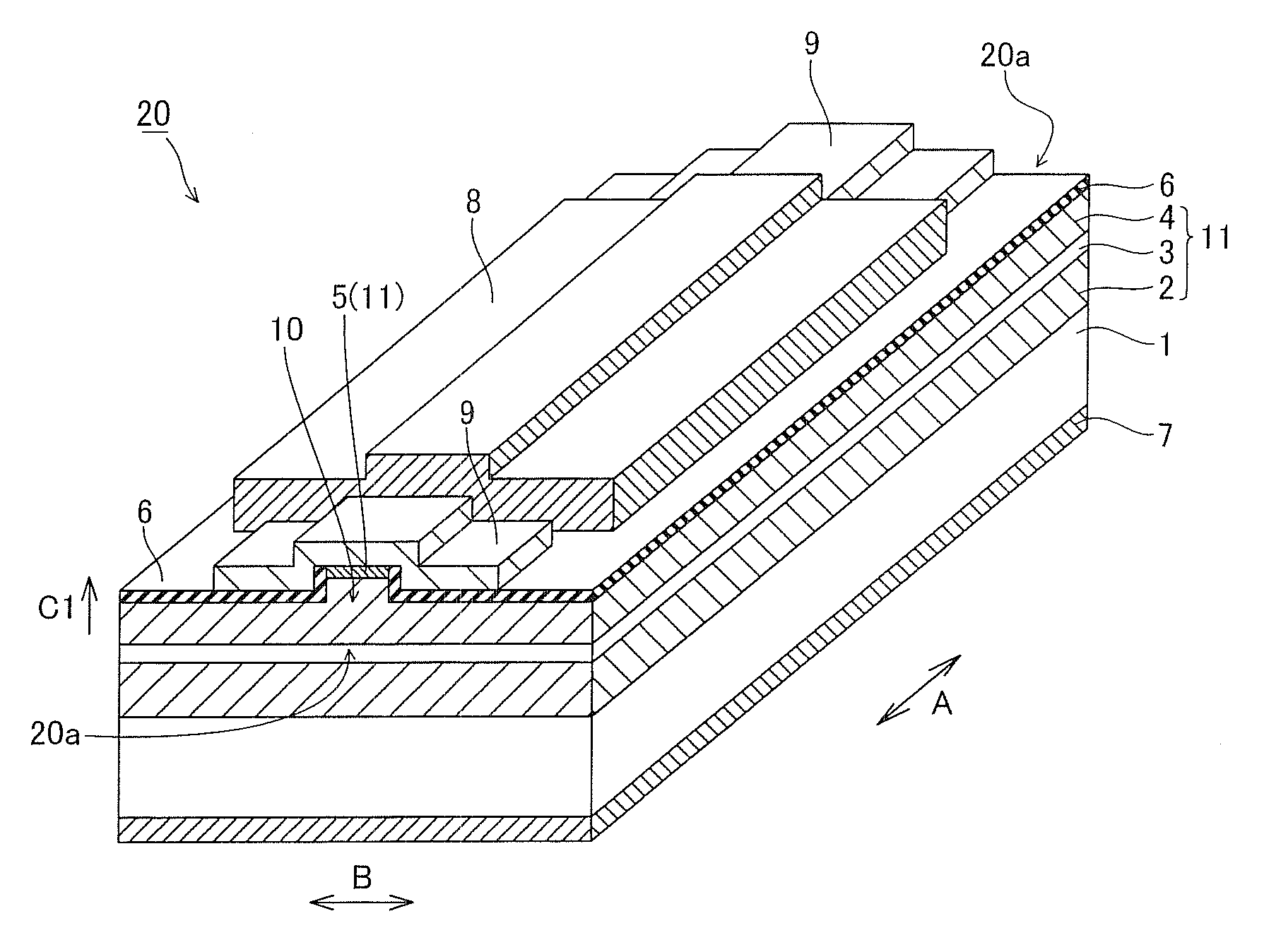
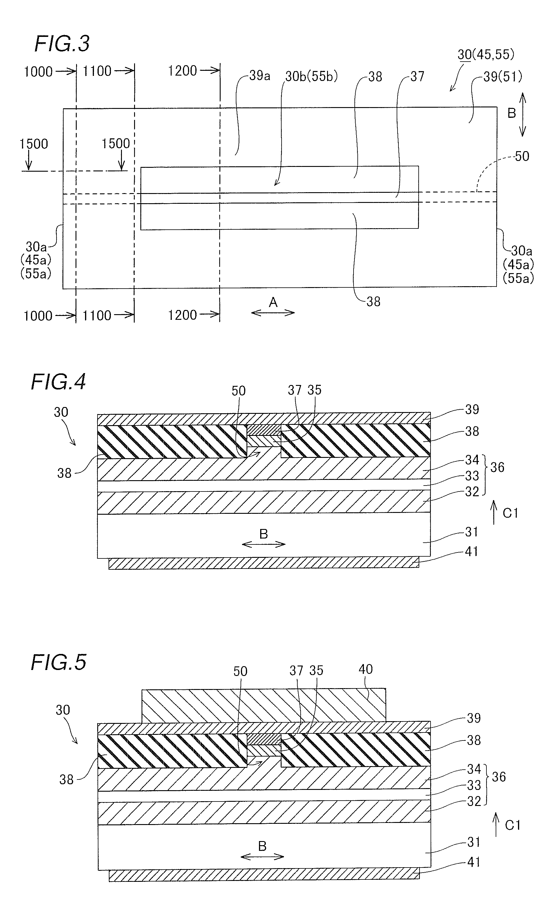
[0126]Referring to FIGS. 3 and 13, a facet protective film 46a is formed on a cavity facet 45a in a semiconductor laser device 45 according to a modification of the first embodiment, dissimilarly to the aforementioned first embodiment. FIG. 13 shows a cross section taken along the line 1500-1500 in FIG. 3.
[0127]According to the modification of the first embodiment, the facet protective film 46a made of an AlN film having a thickness of about 10 nm and an Al2O3 having a thickness of about 80 nm successively from the cavity facet 45a is formed on the cavity facet 45a on a light emitting side, as shown in FIG. 13. A facet protective film 46b made of a SiO2 / ZrO2 multiply-stacked layer, having a total thickness of about 600 nm is formed on a cavity facet 45b on a side opposite to the cavity facet 45a on the light emitting side. The facet protective films 46a and 46b are formed on upper ends (along arrow C1) of the cavity facets 45a and 45b respectively to ...
second embodiment
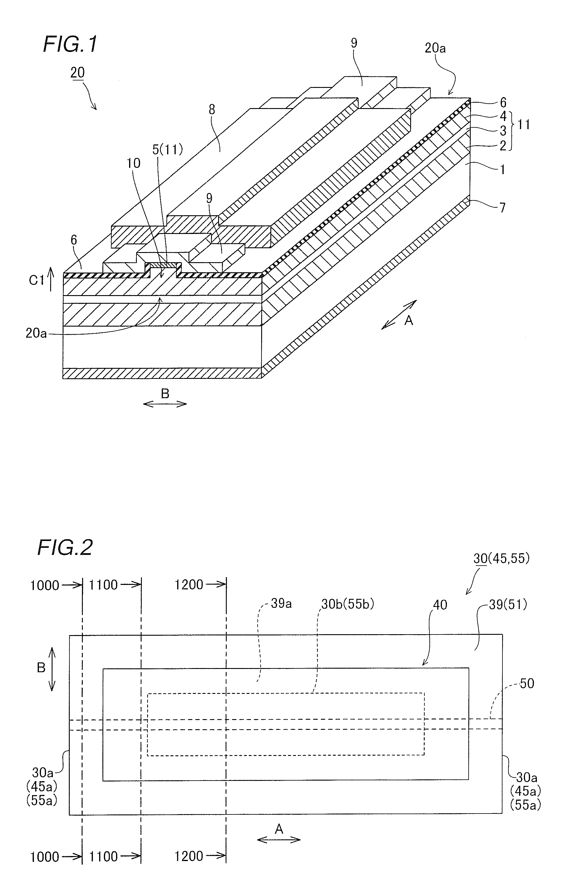
[0130]Referring to FIGS. 2 and 14 to 16, a thermal conductive film 51 made of a material different from a thermal conductive film 39 is further formed on a surface of the thermal conductive film 39 in a semiconductor laser device 55 according to a second embodiment, dissimilarly to the aforementioned first embodiment. FIG. 14 shows a cross section taken along the line 1000-1000 in FIG. 2, and FIG. 15 shows a cross section taken along the line 1100-1100 in FIG. 2. FIG. 16 shows a cross section taken along the line 1200-1200 in FIG. 2.
[0131]According to the second embodiment, the thermal conductive film 51 made of SiO2 is formed on the surface of the thermal conductive film 39 made of Si, as shown in FIGS. 14 to 16. The thermal conductive film 39 has a thickness of about 150 nm and the thermal conductive film 51 has a thickness of about 100 nm. Therefore, the p-side pad electrode 40 is formed to continuously cover the thermal conductive film 51 in a direction B at a position shown in ...
third embodiment
[0139]Referring to FIGS. 19 to 22, a current blocking layer 61 having a prescribed thickness is formed on side surfaces of a ridge 50 and a planar portion of a p-type cladding layer 34 in a semiconductor laser device 60 according to a third embodiment, dissimilarly to the aforementioned second embodiment.
[0140]FIG. 20 shows a cross section taken along the line 3000-3000 in FIG. 19, and FIG. 21 shows a cross section taken along the line 3100-3100 in FIG. 19. FIG. 22 shows a cross section taken along the line 3200-3200 in FIG. 19.
[0141]According to the third embodiment, the current blocking layer 61 made of SiO2, having the prescribed thickness is formed on the side surfaces of the ridge 50 and the planar portion of the p-type cladding layer 34 as shown in FIGS. 20 to 22. Therefore, at a position (cross section taken along the line 3000-3000 in FIG. 19) shown in FIG. 20, a thermal conductive film 62 made of Si and a thermal conductive film 63 made of SiO2 are formed to protrude in a c...
PUM
 Abstract
Description
Claims
Application Information