Monitoring test element groups (TEGS) for etching process and methods of manufacturing a semiconductor device using the same

a technology of etching process and semiconductor device, which is applied in the direction of individual semiconductor device testing, semiconductor/solid-state device testing/measurement, instruments, etc., can solve the problems of difficult to measure the depth of the etched partial via contact hole, and the difficulty of confirming the accuracy of the etched contact hole depth while performing the etching process of the contact hole and trench, etc., to achieve accurate measurement

Active Publication Date: 2012-09-13
SAMSUNG ELECTRONICS CO LTD
View PDF4 Cites 8 Cited by
  • Summary
  • Abstract
  • Description
  • Claims
  • Application Information

AI Technical Summary

Benefits of technology

[0027]In example embodiments, a depth of a partial via contact hole may be accurately measured using a TEG in accordance with the present inventive concept. Using the measured depth of the partial via contact hole, the partial via contact hole may be evaluated if formed normally. Accordingly, process defects generated due to formation of an abnormal partial via contact hole may be prevented.

Problems solved by technology

However, confirmation of the contact hole etched having an accurate depth while performing the forming process of a contact hole and a trench may not be an easy task.
For example, when an insulating interlayer is not etched to an etch stopping layer at one time but is partially etched to form a partial via contact hole first while forming a contact hole, the measuring of a depth of the etched partial via contact hole may be a difficult task.

Method used


Image

  • Monitoring test element groups (TEGS) for etching process and methods of manufacturing a semiconductor device using the same
  • Monitoring test element groups (TEGS) for etching process and methods of manufacturing a semiconductor device using the same
  • Monitoring test element groups (TEGS) for etching process and methods of manufacturing a semiconductor device using the same

Examples


Embodiment Construction

[0035]Various example embodiments will be described more fully hereinafter with reference to the accompanying drawings, in which some example embodiments are shown. Example embodiments of the present inventive concept may, however, be embodied in many different forms and should not be construed as limited to example embodiments set forth herein. In the drawings, the sizes and relative sizes of layers and regions may be exaggerated for clarity.

[0036]It will be understood that when an element or layer is referred to as being “on,”“connected to” or “coupled to” another element or layer, it can be directly on, connected or coupled to the other element or layer or intervening elements or layers may be present. Like numerals refer to like elements throughout. As used herein, the term “and / or” includes any and all combinations of one or more of the associated listed items.

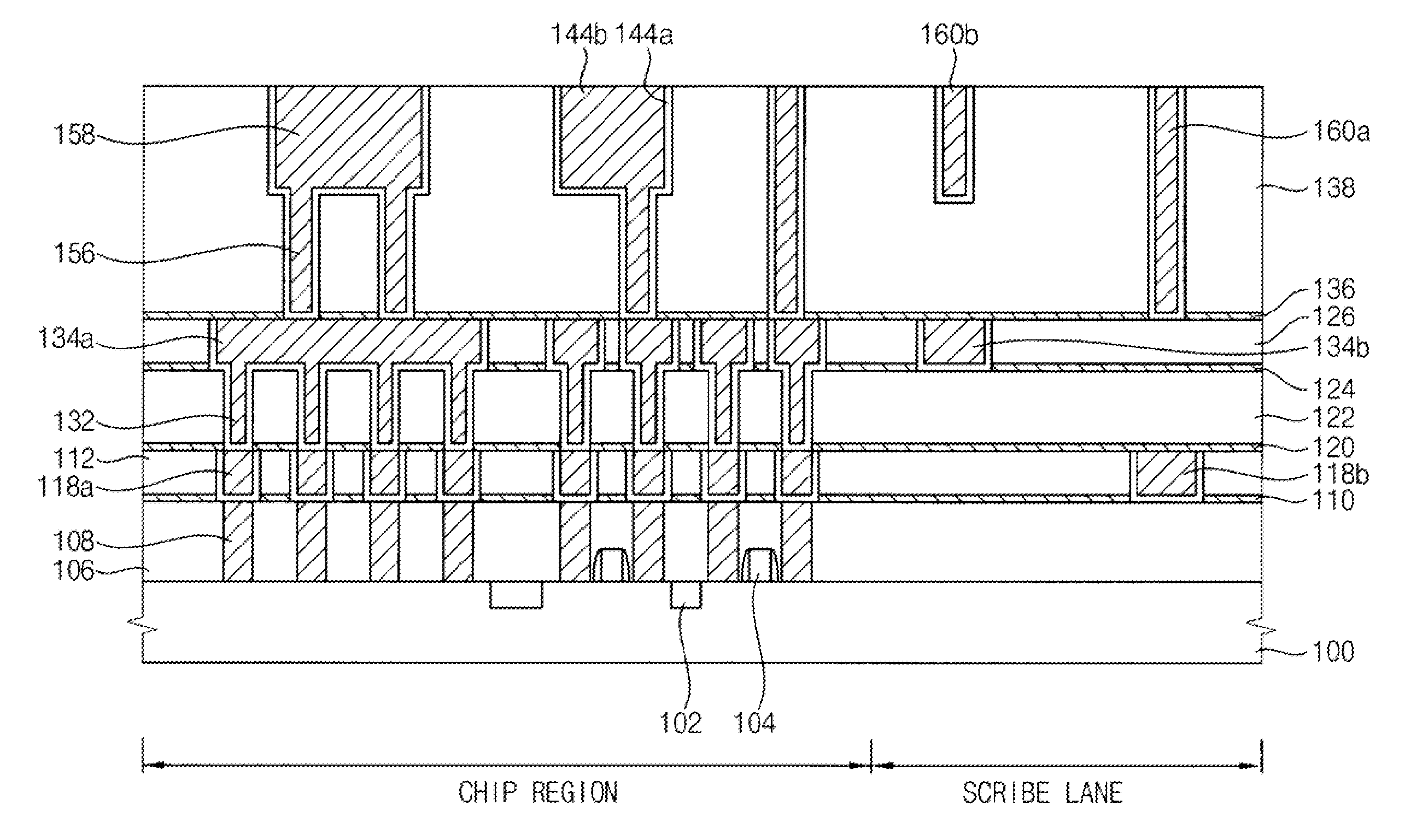
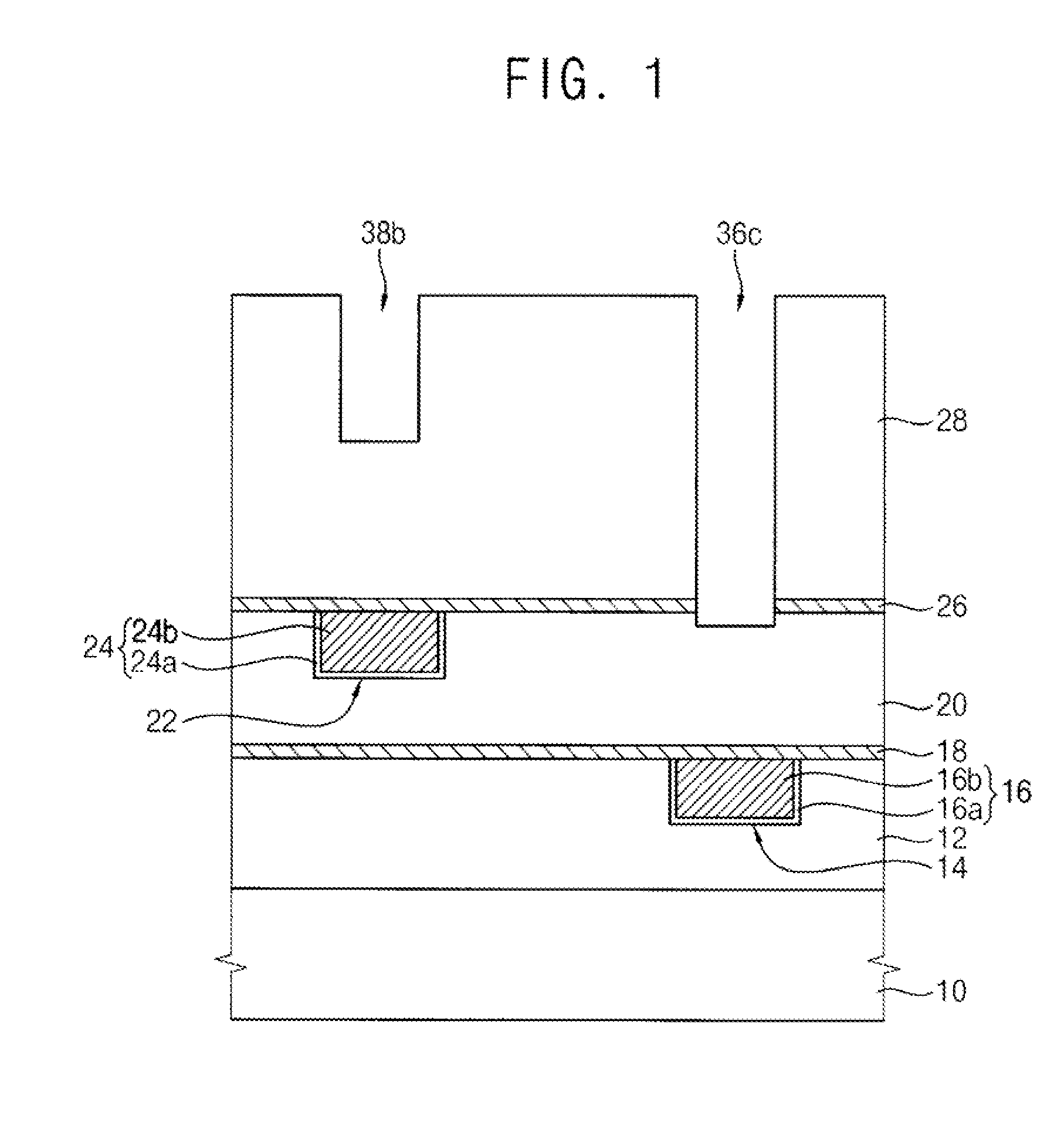
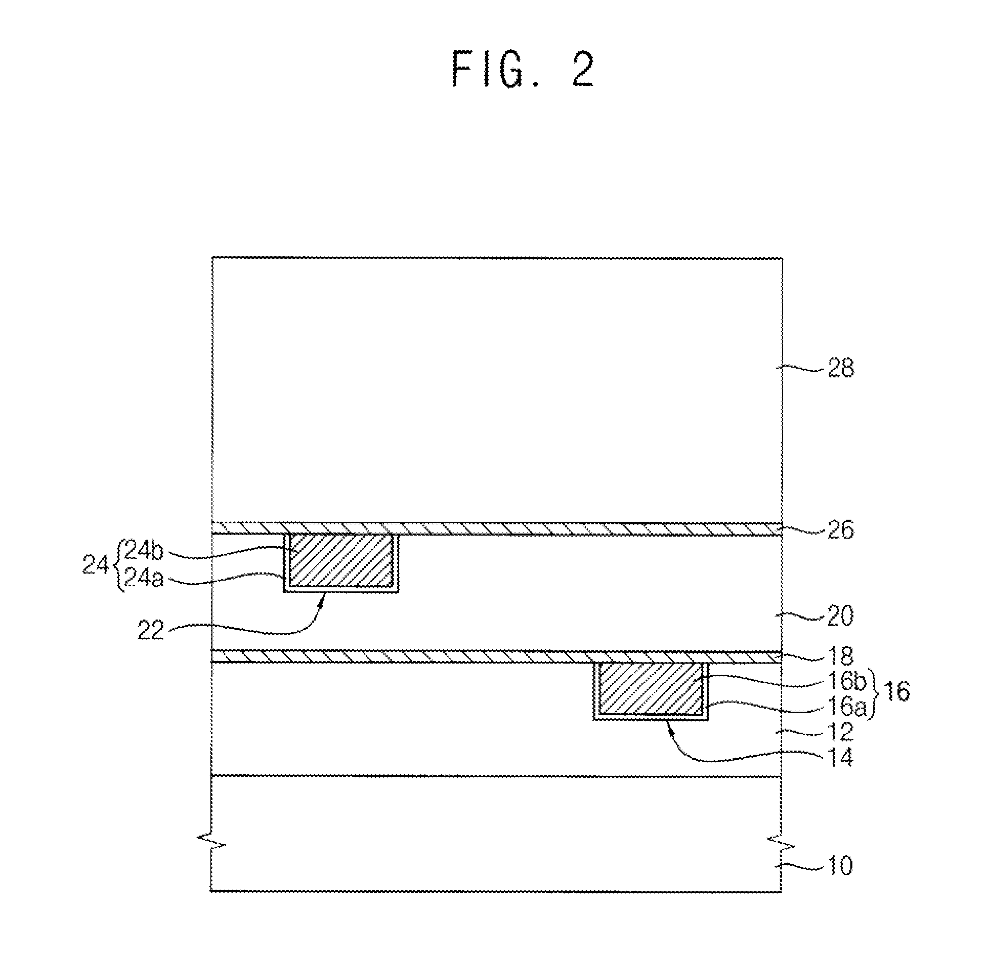
[0037]Hereinafter, example embodiments on monitoring TEGs for an etching process and methods of manufacturing a semicon...


PUM


Abstract

Disclosed is a monitoring TEG for an etching process in a semiconductor device. The TEG includes an etch stopping layer on a substrate and a target layer to be etched provided on the etch stopping layer. The target layer to be etched includes a first opening portion formed by etching a portion of the target layer to be etched and a second opening portion formed by etching another portion of the target layer to be etched. The second opening portion has a smaller depth than the first opening portion. A depth of a partial contact hole formed by a first partial etching process may be measured.

Description

CROSS-REFERENCE TO RELATED APPLICATIONS[0001]This application claims priority under 35 USC §119 to Korean Patent Application No. 10-2011-0021009, filed on Mar. 9, 2011, the disclosure of which is hereby incorporated by reference herein in it's entirety.BACKGROUND[0002]1. Technical Field[0003]Example embodiments relate to monitoring TEGs for an etching process and methods of manufacturing a semiconductor device using the same. More particularly, example embodiments relate to monitoring TEGs for an etching process for accurately measuring a depth of a contact hole formed while performing a partial etching process for forming a metal wiring and methods of manufacturing a semiconductor device using the same.[0004]2. Description of the Related Art[0005]To form a metal contact and a wiring line in a semiconductor device, a contact hole and a trench may be formed in advance. In addition, a depth of the contact hole etched may be required to be measured accurately. However, confirmation of ...

Claims


Application Information

Patent Timeline
Patent Type & Authority Applications(United States)
IPC IPC(8): H01L21/66
CPCH01L22/12H01L2924/0002H01L2924/00H01L21/76811H01L21/3213H01L21/76829H01L22/34
Inventor LEE, KYOUNG-WOOSHIN, HONG-JAEJANG, WOO-JIN
Owner SAMSUNG ELECTRONICS CO LTD
Why Eureka
Try Eureka