Programmable test chip, system and method for characterization of integrated circuit fabrication processes

Active Publication Date: 2012-09-27
RIDGETOP GROUP
View PDF19 Cites 14 Cited by
  • Summary
  • Abstract
  • Description
  • Claims
  • Application Information

AI Technical Summary

Benefits of technology

[0010]The present invention provides a test chip, system and method for testing large numbers of test devices on a single test chip to characterize an IC fabrication process, decreasing the time and complexity required to characterize the variation and reliability of the IC fabrication process. This is accomplished with a remotely configurable test chip that can b

Problems solved by technology

Device degradation will accumulate over time and with use and results in a continuous change in the electrical properties of transistors.
Modern nanotechnology CMOS circuits have numerous reliability concerns that have to be accounted for during design and verification cycles.
The

Method used


Image

  • Programmable test chip, system and method for characterization of integrated circuit fabrication processes
  • Programmable test chip, system and method for characterization of integrated circuit fabrication processes
  • Programmable test chip, system and method for characterization of integrated circuit fabrication processes

Examples


Embodiment Construction

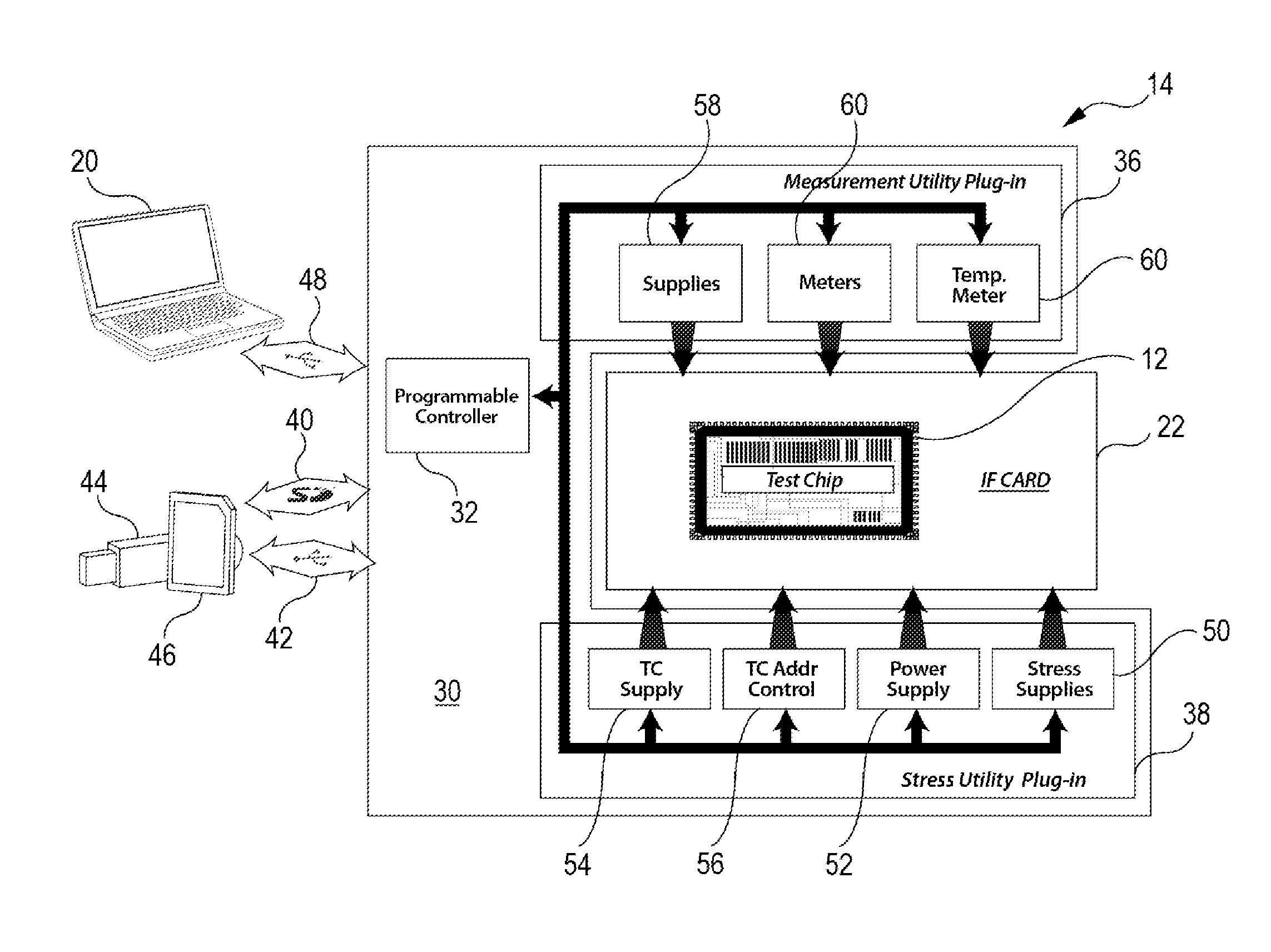
[0028]The present invention provides a test chip, system and method for testing large numbers of test devices on a single test chip to characterize an IC fabrication process, decreasing the time and complexity required to characterize the variation and reliability of the IC fabrication process. This is accomplished with a remotely configurable test chip that can be programmed with varying bias conditions for testing of process variation or numerous failure modes on large sample sizes. An on-chip addressing technique allows large numbers of test devices to be tested simultaneously and the measurement signals read out serially for different test devices. The test chip may be configured for wafer, die or package-level testing. Without loss of generality, embodiments of the test chip will be described for package-level testing. The term “contact” may be used to refer to contact pads on the die or the external pins of the package.

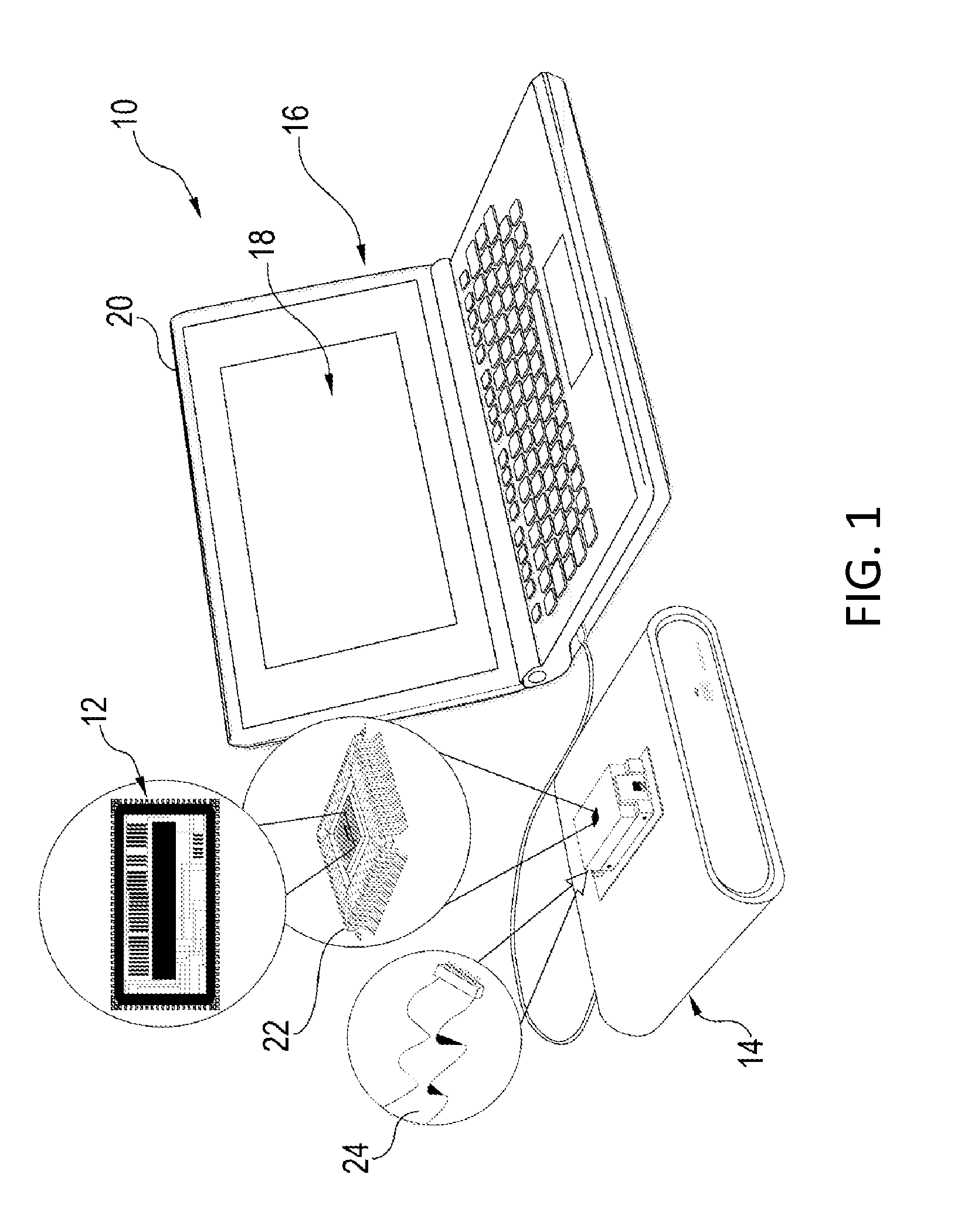
[0029]Referring now to FIG. 1, a test system 10 includes a...


PUM


Abstract

A test chip, system and method for testing large numbers of test devices on a single test chip decreases the time and complexity required to characterize the variation and reliability of the IC fabrication process. A remotely configurable test chip can be programmed with varying bias conditions for testing of process variation or numerous failure modes on large sample sizes. An on-chip addressing technique allows large numbers of test devices to be tested simultaneously and the measurement signals read out serially for different test devices. The test chip may be configured for wafer, die or package-level testing.

Description

CROSS-REFERENCE TO RELATED APPLICATIONS[0001]This application claims benefit of priority under 35 U.S.C. 119(e) to U.S. Provisional Application No. 61 / 465,463 entitled “Method and System for Intrinsic Reliability Characterization of Integrated Circuit Fabrication Processes” and filed on Mar. 21, 2011, the entire contents of which are incorporated by reference.BACKGROUND OF THE INVENTION[0002]1. Field of the Invention[0003]This invention relates to reliability characterization of integrated circuit (IC) fabrication processes, and more particularly to a programmable test chip, system and method for characterization of process variation and reliability of IC fabrication processes at the wafer, die or package levels.[0004]2. Description of the Related Art[0005]Increasing the performance of integrated circuits (ICs) requires a complete and accurate characterization of the variation and reliability of available IC fabrication processes. Established processes must be characterized to provi...

Claims


Application Information

Patent Timeline
IPC IPC(8): G06F19/00G16H40/40G16H40/67G16Z99/00
CPCG06F19/00G01R31/2884H01L22/34G16H40/40G16H40/67G16Z99/00B01L2300/0825
Inventor MIKKOLA, ESKO O.
Owner RIDGETOP GROUP
Why Eureka
Try Eureka