Silicon carrier space transformer and temporary chip attach burn-in vehicle for high density connections

Active Publication Date: 2012-10-04
IBM CORP
View PDF2 Cites 11 Cited by
  • Summary
  • Abstract
  • Description
  • Claims
  • Application Information

AI Technical Summary

Benefits of technology

[0016]The present invention will become readily apparent to those of ordinary skill in the art when

Problems solved by technology

Although this technology is utilized for area array contacts and to penetrate a bump or pad for electrical test, since it does not scale to very small scale pitch area pad and bump contacts while maintaining dimensional stability at both time zero for testing and throughout the life of testing, it does not lend itself to the dense arrays of pads and bumps.
Each wire is rigid enough to apply pressure, and the mechanical assembly of the wires can provide testing but is limited due to capacitance and inductance as well as center-to-center pitch of probe contacts to test an array or pads and / or bumps.
The performance of Buckling Beam Probes is limited due to capacitance, inductance and pitch spacing to pads and / or bumps.
Contact structures, which can support perimeter pad connections and array connections to pads or bumps at a large spacing while maintaining springable shape, have been developed but have limitations in pitch and electrical parasitics which limit its use.

Method used


Image

  • Silicon carrier space transformer and temporary chip attach burn-in vehicle for high density connections
  • Silicon carrier space transformer and temporary chip attach burn-in vehicle for high density connections
  • Silicon carrier space transformer and temporary chip attach burn-in vehicle for high density connections

Examples


Embodiment Construction

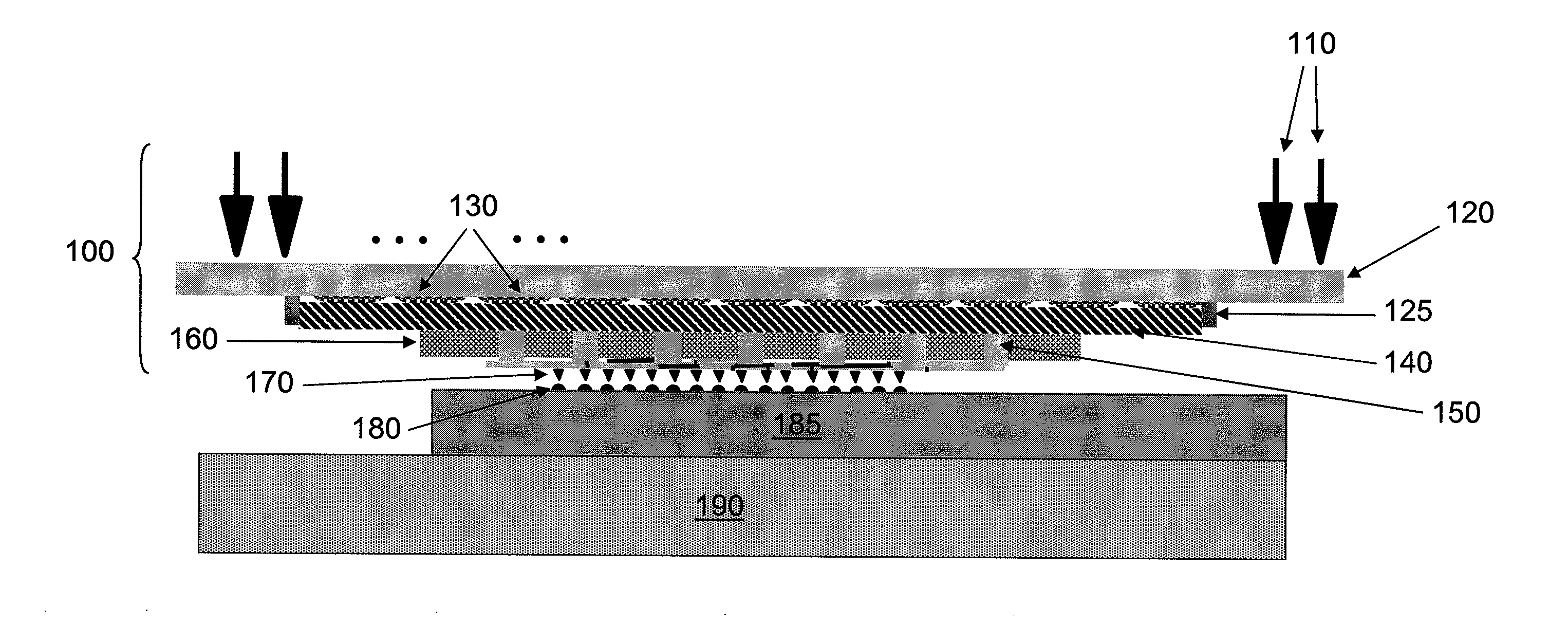
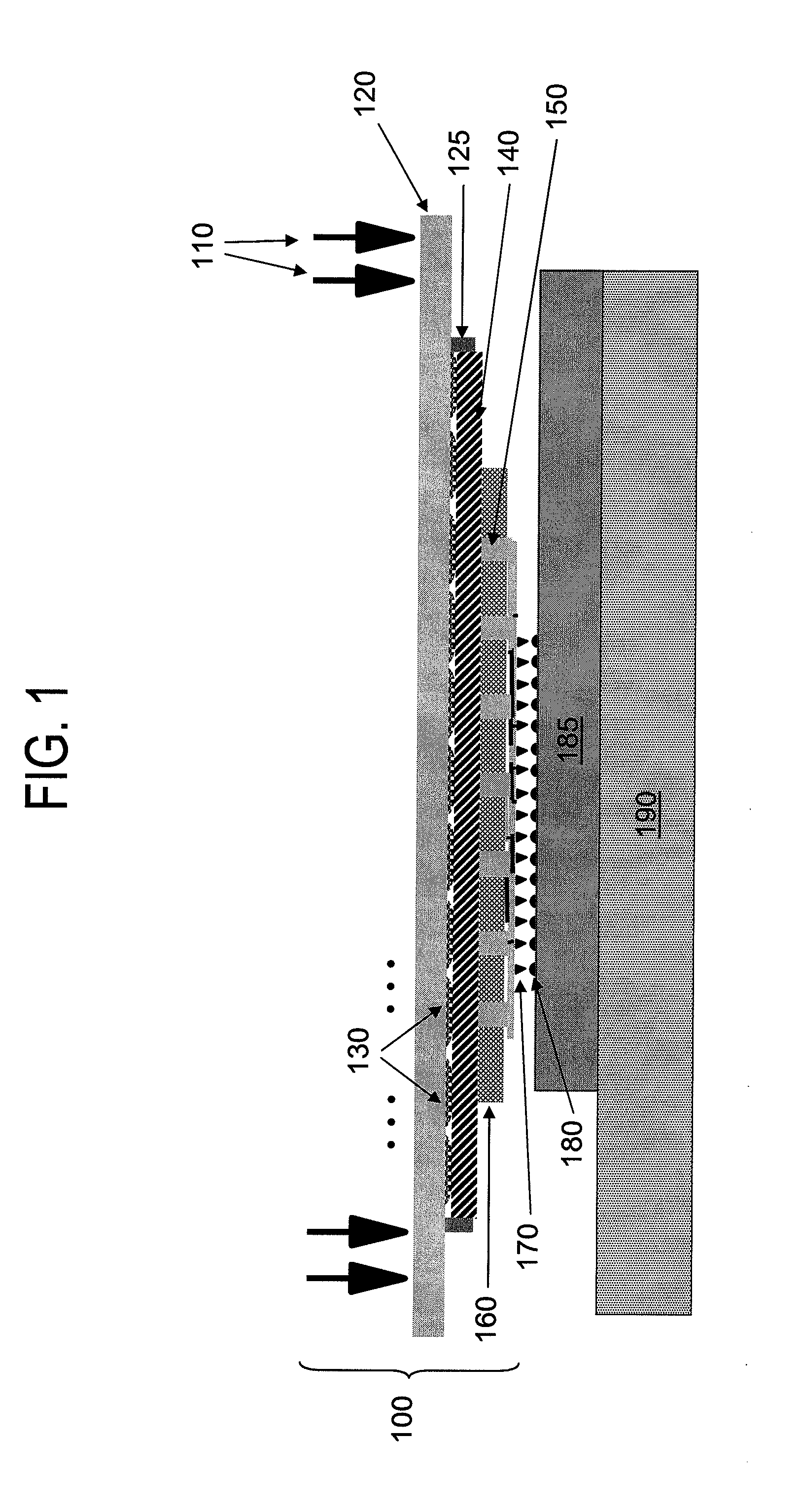
[0024]Hereinafter, exemplary embodiments of the present invention will be described with reference to the accompanying drawings.

[0025]Various exemplary embodiments of the present invention include a space transformer to support high I / O interconnection, test and / or burn-in, with integrated function such as decoupling capacitors built into the silicon space transformer and probes for enhanced function test, enhanced throughput and lower costs.

[0026]Various exemplary embodiments of the present invention include a silicon based space transformer and test probes that may be cost effectively scaled using ceramic based, thin film based or probe card based technologies. A silicon based space transformer, according to an exemplary embodiment of the present invention, includes wafer scale wiring dimensions that permit I / O interconnection and test probes that can permit about 104 connections / cm2 to about 105 connections / cm2 to over 106 connections / cm2.

[0027]Using a silicon based test probe or...


PUM


Abstract

A silicon carrier space transformer assembly includes one or more silicon structures, which provide space transformer scaling to permit interconnection for fine pitch input / output interconnections with a semiconductor die or wafer, and fine pitch test probe tips connected to the one or more silicon structures.

Description

FEDERALLY SPONSORED RESEARCH AND DEVELOPMENT [0001]This invention was made with Government support under Contract No. NBCHC020056 and MDA972-03-3-0004 awarded by Defense Advanced Research Projects Agency (DARPA). The Government has certain rights in this invention.BACKGROUND OF THE INVENTION[0002]1. Technical Field[0003]The present disclosure relates to semiconductor microelectronics and, more particularly, to test hardware probes, space transformers and structures, and test methods which enable test and burn-in for semiconductor wafers, die, die stacks or other semiconductor and packaging hardware.[0004]2. Discussion of Related Art[0005]Semiconductor chips and wafers support an increasing number of transistors as each new generation of semiconductor technology leverages the ability to use smaller device feature sizes produced from more advanced lithography. Advances in semiconductor technology have contributed to the reduction in the size and cost of chips and helped to improve cos...

Claims


Application Information

Patent Timeline
IPC IPC(8): G01R1/067
CPCG01R31/2889G01R31/2893H01L28/40H01L21/76885H01L28/10G01R31/2894
Inventor HAMEL, HARVEYKNICKERBOCKER, JOHN ULRICHMCKNIGHT, SAMUELPATEL, CHIRAG S.
Owner IBM CORP
Why Eureka
Try Eureka