
Substrate for fabricating light emitting device and light emitting device fabricated therefrom

Inactive Publication Date: 2012-10-11
EPISTAR CORP
View PDF1 Cites 5 Cited by
  • Summary
  • Abstract
  • Description
  • Claims
  • Application Information

AI Technical Summary

Benefits of technology

[0010]An objective of the present invention is to provide a substrate for fabricating a light emitting device having an improved surface structure provided with a major growth platform to prevent interval defects from generating and having increased effective surface areas of the protruded portions for enhancing the light extraction efficiency.
[0021]The present invention further provides a patterned substrate for fabricating a light emitting device having an improved surface structure, comprising: at least one platform region serving as a primary platform for epitaxial growth; and a plurality of directly adjacent protruded portions surrounding the at least one platform region to isolate the at least one platform region from another platform region so as to enhance light extraction efficiency, each directly adjacent protruded portion having a scattering surface and a vertex, wherein at least one unit region is surrounded by the vertexs or lines between the adjacent vertexs of the plural directly adjacent protruded portions, an area of the unit region consists of an area of the protruded portions and an area of the platform region, the area of the protruded portion is larger than the area of the platform region.

Problems solved by technology

However, for one skilled in the art, it is generally known that the poor quantum efficiency (external or internal) of LED may result in transferring the energy which has not been successfully converted into light into heat, and if the heat has not been properly dissipated from LED effectively, it may subsequently result in raising the temperature of LED and reducing the light emitting efficiency.
When light travels through these interval defects with irregular shapes, light will be directed into and restricted within the defects so as to reduce the external quantum efficiency.
Solutions to these problems have been long sought but prior developments have not taught or suggested any solutions and, thus, solutions to these problems have long eluded those skilled in the art.

Method used


Image

  • Substrate for fabricating light emitting device and light emitting device fabricated therefrom
  • Substrate for fabricating light emitting device and light emitting device fabricated therefrom
  • Substrate for fabricating light emitting device and light emitting device fabricated therefrom

Examples


Embodiment Construction

[0040]The following embodiments are described in sufficient detail to enable those skilled in the art to make and use the invention. It is to be understood that other embodiments would be evident based on the present disclosure, and that process and mechanical changes may be made without departing from the scope of the present invention.

[0041]In the following description, numerous specific details are given to provide a thorough understanding of the invention. However, it will be apparent that the invention may be practiced without these specific details. In order to avoid obscuring the present invention, some well-known configurations and process steps are not disclosed in detail.

[0042]In the following description, several examples are given to provide a thorough understanding of the patterned substrate of the invention.

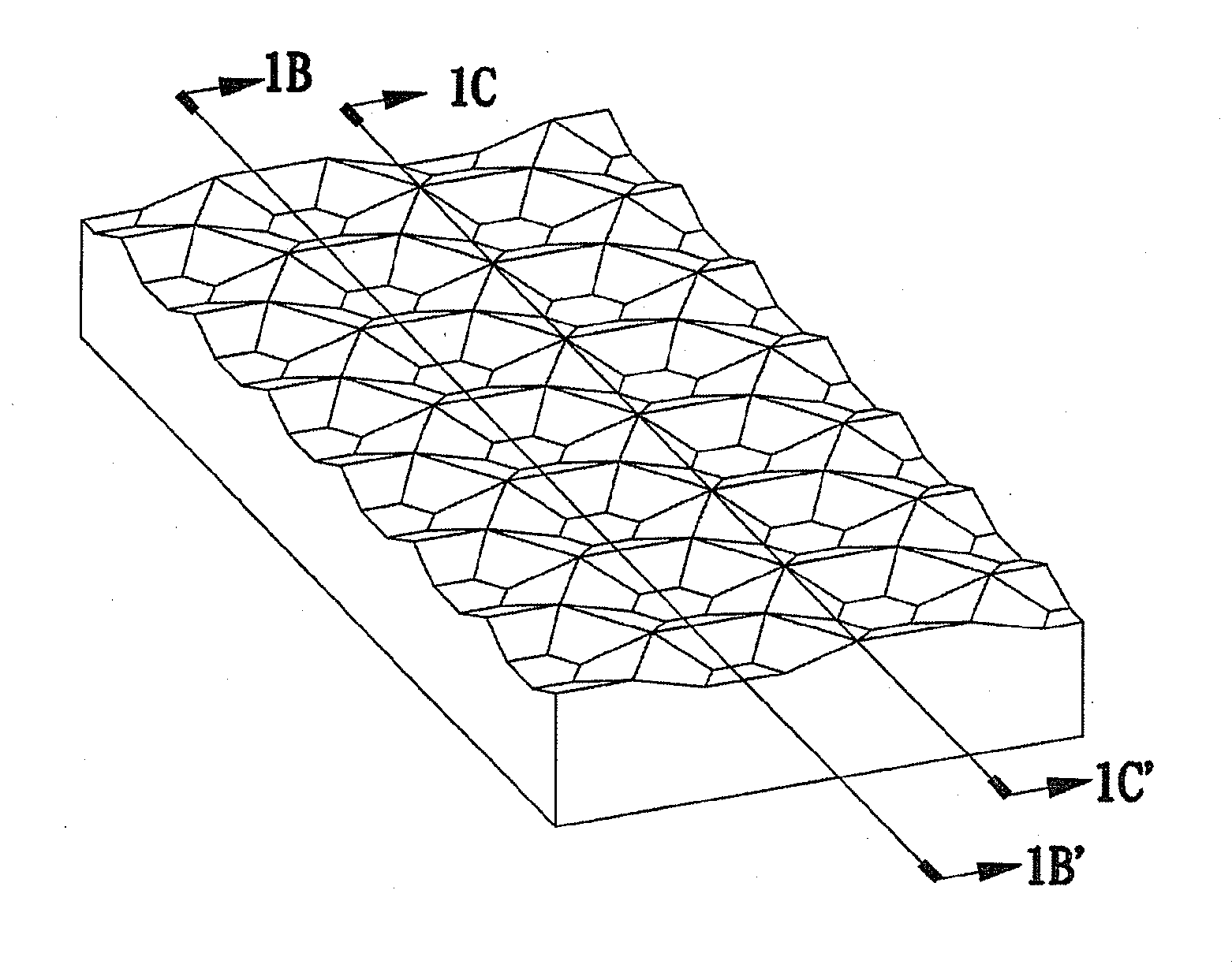
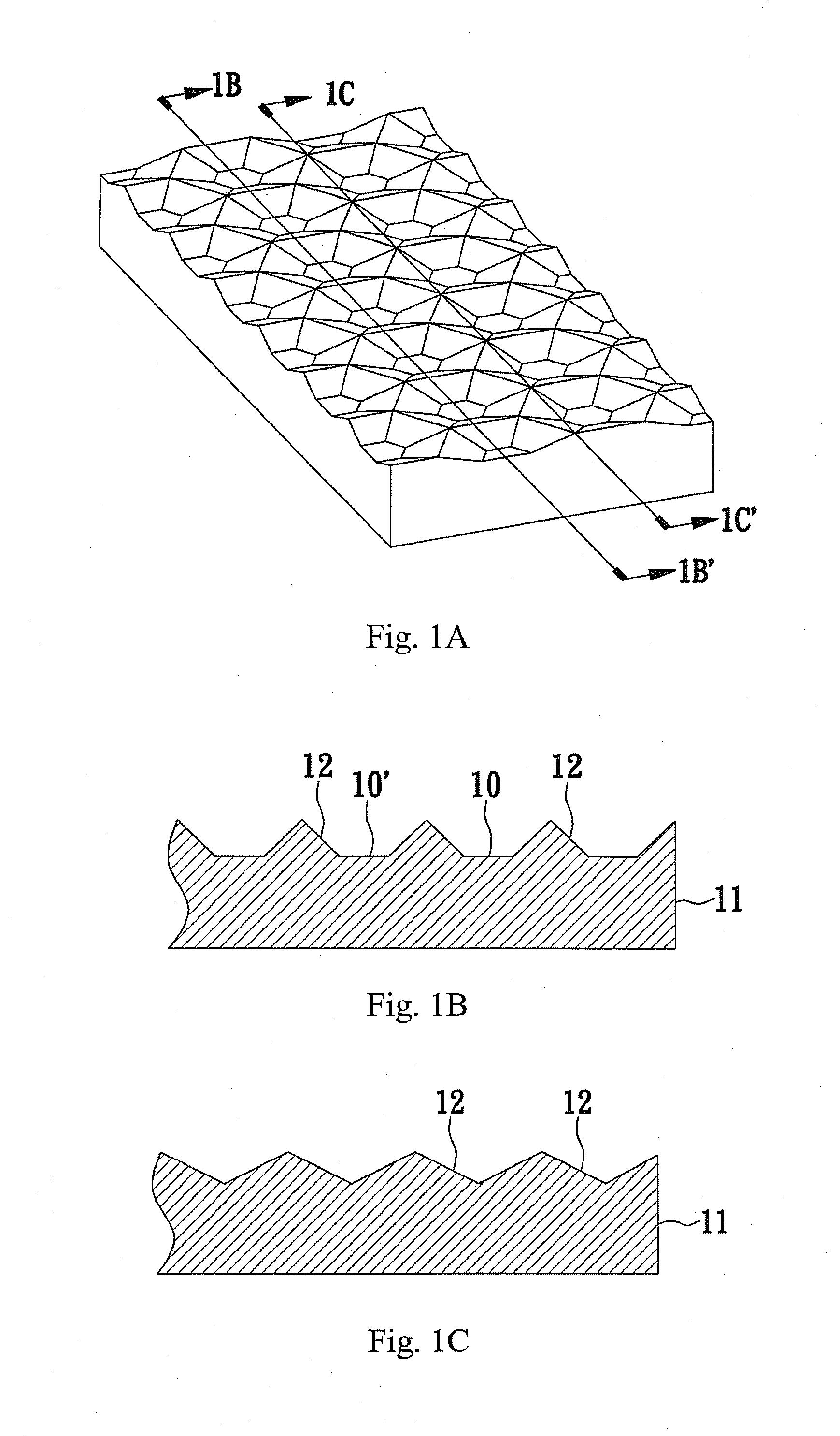
[0043]FIGS. 1A to 1C illustrate an embodiment of the patterned substrate of the invention. FIG. 1A is a perspective view of a preferred embodiment of the patterned ...


PUM


Abstract

The invention provides a patterned substrate for fabricating a light emitting device having an improved surface structure and the light emitting device fabricated therefrom. The patterned substrate includes at least one platform region having a first facet direction for epitaxial growth; and a plurality of directly adjacent protruded portions surrounding the at least one platform region to isolate the at least one platform region from another platform region, wherein facet direction of each scattering surface of the plurality of directly adjacent protruded portions is substantially excluded from first facet direction. Since facet direction of each scattering surface of the plurality of directly adjacent protruded portions substantially do not include the first facet direction, during formation of the light emitting device, epitaxial growth is mainly conducted on the at least one platform region, which may prevent epitaxial defects from generating and enhance external quantum efficiency of the light emitting device.

Description

CROSS-REFERENCE TO RELATED APPLICATION[0001]This application is a continuation-in-part of and claims the priority benefit of U.S. application Ser. No. 12 / 453,409, filed on May 11, 2009, now pending, which claims the priority benefit of Taiwan application serial no. 097126565, filed on Jul. 14, 2008. The entirety of each of the above-mentioned patent applications is hereby incorporated by reference herein and made a part of this specification.FIELD OF THE INVENTION[0002]The present invention relates generally to a substrate for fabricating a light emitting device and the light emitting device fabricated therefrom. More particularly, the present invention relates to a patterned substrate for fabricating a light emitting diode (LED) and the LED with high light extraction efficiency fabricated therefrom.BACKGROUND OF THE INVENTION[0003]In recent years, a light emitting device, or a light emitting diode (LED), has been widely used in the applications such as back lights of displays or li...

Claims


Application Information

Patent Timeline
IPC IPC(8): B32B3/30
CPCC30B25/18C30B29/20C30B29/406Y10T428/24479H01L33/22H01L31/02366Y02E10/50H01L33/16
Inventor CHENG, CHIH-CHING
Owner EPISTAR CORP
Features
  • Generate Ideas
  • Intellectual Property
  • Life Sciences
  • Materials
  • Tech Scout
  • Unparalleled Data Quality
  • Higher Quality Content
  • 60% Fewer Hallucinations
Learn More