

Display device
- Summary
- Abstract
- Description
- Claims
- Application Information
AI Technical Summary
Benefits of technology
Problems solved by technology
Method used
Image

Examples
first embodiment
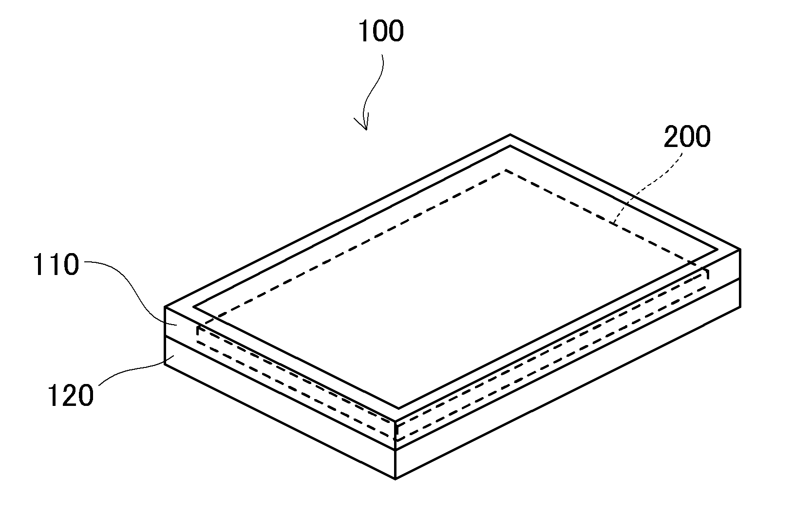
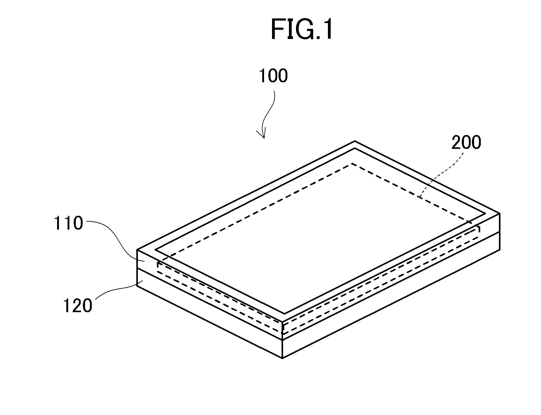
[0038]FIG. 1 schematically shows a liquid crystal display device 100 according to an embodiment of the present invention. As shown in FIG. 1, the liquid crystal display device 100 includes a liquid crystal panel 200 which is fixed in place between an upper frame 110 and a lower frame 120, a backlight device (not shown), and the like.
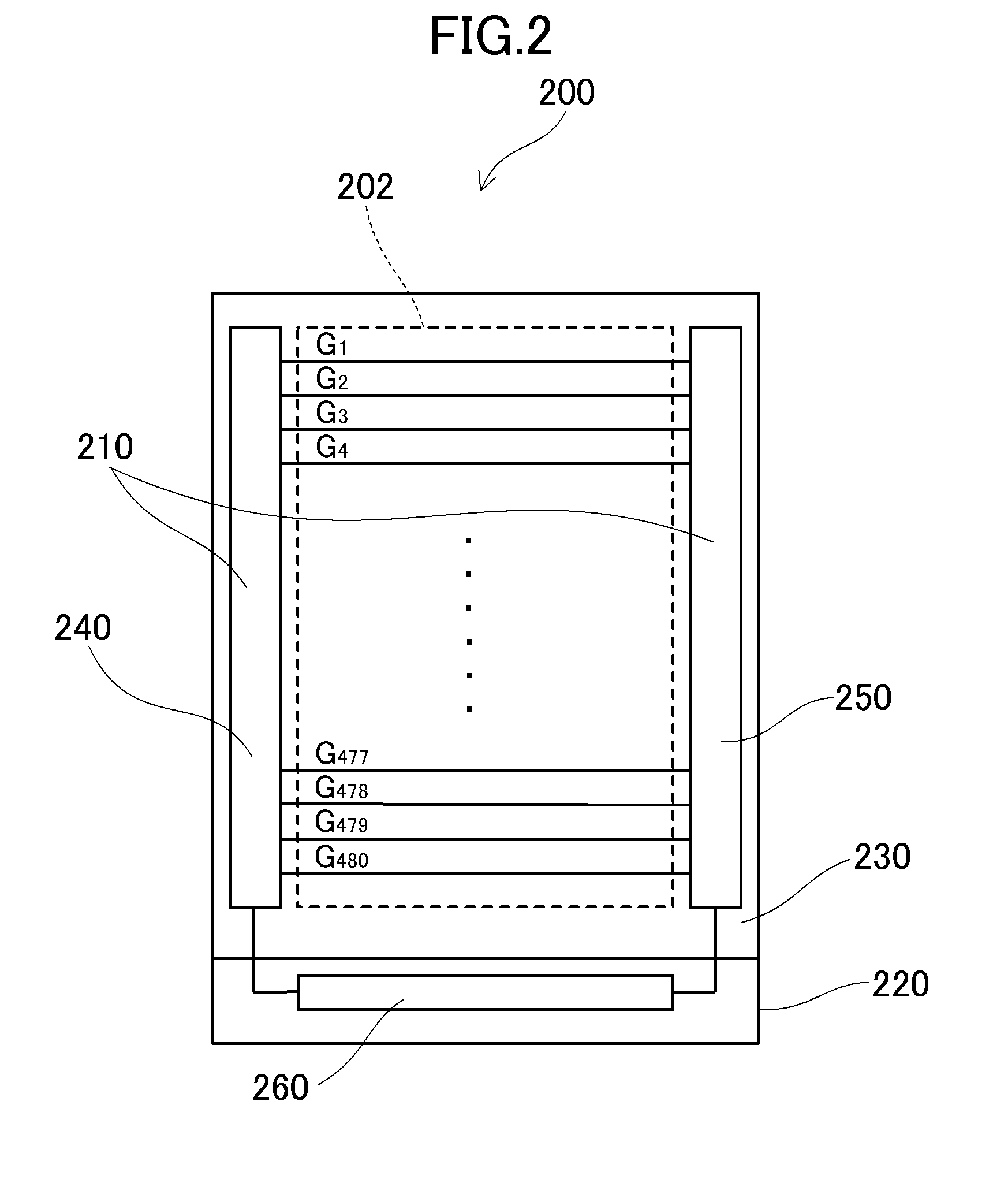
[0039]FIG. 2 shows a configuration of the liquid crystal panel 200 shown in FIG. 1. The liquid crystal panel 200 includes two substrates of a TFT (Thin Film Transistor) substrate 220 and a color filter substrate 230, and liquid crystal composition is sealed between the two substrates. The TFT substrate 220 includes a driving circuit 210 which sequentially applies predetermined voltages to scanning signal lines G1 to G480, and a driving IC (Integrated Circuit) 260 which applies voltages corresponding to grayscale values of pixels to a plurality of data signal lines (not shown) which extend so as to perpendicularly intersect the scanning signal lines G1 to...
second embodiment
[0047]The second embodiment of the present invention will be described. A configuration of the liquid crystal display device according to the second embodiment is the same as the configuration according to the first embodiment shown in FIG. 1, and thus a redundant description will be omitted.
[0048]FIG. 7 shows a liquid crystal panel 300 of the liquid crystal display device according to the second embodiment. The liquid crystal panel 300 includes two substrates of a TFT substrate 320 and a color filter substrate 330, and liquid crystal composition is sealed between the two substrates. The TFT substrate 320 includes a driving circuit 310 which sequentially applies predetermined voltages to scanning signal lines G1 to G480, and a driving IC 360 which applies voltages corresponding to grayscale values of pixels to a plurality of data signal lines (not shown) which extend so as to perpendicularly intersect the scanning signal lines G1 to G480 in a pixel region 302 and controls a first ma...
third embodiment
[0054]The third embodiment of the present invention will be described. A configuration of the liquid crystal display device according to the third embodiment is the same as the configuration according to the first embodiment shown in FIG. 1, and repeated description will be omitted.
[0055]FIG. 13 shows a liquid crystal panel 400 of the liquid crystal display device according to the third embodiment. The liquid crystal panel 400 includes two substrates of a TFT substrate 420 and a color filter substrate 430, and liquid crystal composition is sealed between the two substrates. The TFT substrate 420 includes a driving circuit 410 which sequentially applies predetermined voltages to scanning signal lines G1 to G480, and a driving IC 460 which applies voltages corresponding to grayscale values of pixels to a plurality of data signal lines (not shown) which extend so as to perpendicularly intersect the scanning signal lines G1 to G480 in a pixel region 402 and controls a first driving circ...
PUM
 Abstract
Description
Claims
Application Information