Light emitting device package and method of manufacturing the same

a technology of light-emitting devices and packaging, which is applied in the manufacture of printed circuits, lighting and heating apparatuses, printed circuit assembling, etc., can solve the problems of increasing the size of chips and requiring more efficient heat-emitting, so as to achieve the effect of maximizing heat-radiation efficiency

Inactive Publication Date: 2012-10-25
SAMSUNG ELECTRONICS CO LTD
View PDF20 Cites 4 Cited by
  • Summary
  • Abstract
  • Description
  • Claims
  • Application Information

AI Technical Summary

Benefits of technology

[0009]An aspect of the present invention provides a light emitting device package in which a bottom surface of a chip is exposed to a lower portion of a package body and comes into direct contact with a mounting substrate, such that heat generated during an operation thereof may be emitted directly to the mounting substrate to thereby allow for maximization of heat radiation efficiency, and a method of manufacturing the same.
[0010]An aspect of the present invention also provides a light emitting device package in which a chip and a wire are sealed through a use of a molding material having excellent mechanical, electrical properties, rather than a sealing material, thereby allowing for an improvement in wire bonding reliability.
[0014]Each of the electrode terminals may include prominences and depressions allowing for enhanced coupling force with the body part, on at least one surface thereof.

Problems solved by technology

However, an increase in the size of a chip may generate a greater amount of heat, as compared to that generated during the operation of a light emitting device chip, such that an attempt at emitting heat more efficiently is required.

Method used


Image

  • Light emitting device package and method of manufacturing the same
  • Light emitting device package and method of manufacturing the same
  • Light emitting device package and method of manufacturing the same

Examples


Embodiment Construction

[0048]Embodiments of the present invention will now be described in detail with reference to the accompanying drawings. The invention may, however, be embodied in many different forms and should not be construed as being limited to the embodiments set forth herein. Rather, these embodiments are provided so that this disclosure will be thorough and complete, and will fully convey the scope of the invention to those skilled in the art.

[0049]In the drawings, the shapes and sizes of components are exaggerated for clarity. The same or equivalent elements are referred to by the same reference numerals throughout the specification.

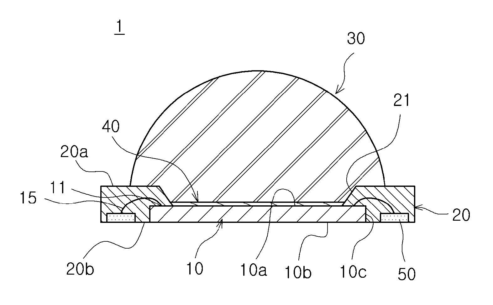
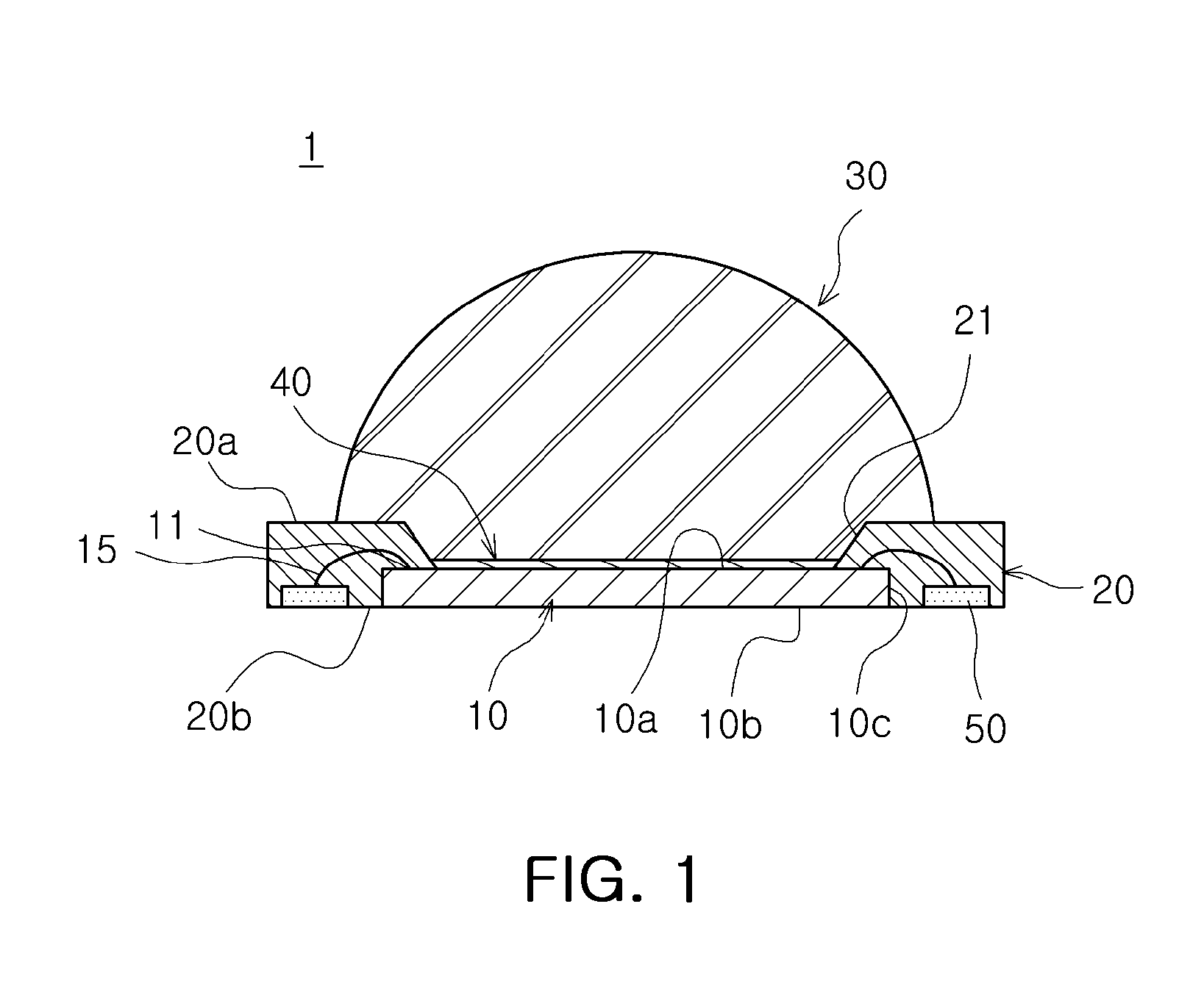
[0050]A light emitting device package according to an embodiment of the present invention will be explained with reference to FIGS. 1 through 4.

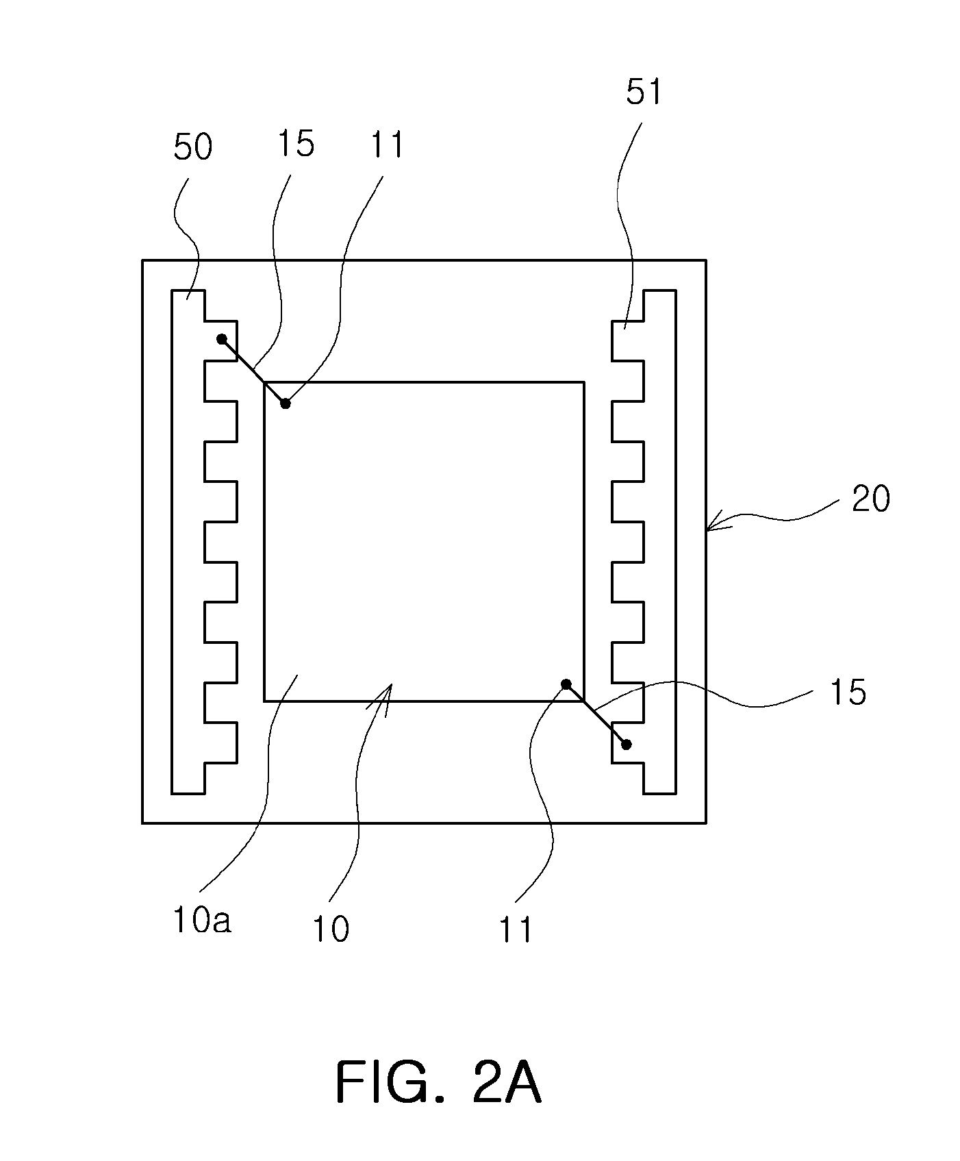
[0051]FIG. 1 is a cross-sectional view schematically showing a light emitting device package according to an embodiment of the present invention. FIGS. 2A and 2B are plan views schematically showing various shapes of an e...


PUM

PropertyMeasurementUnit
sizeaaaaaaaaaa
Tgaaaaaaaaaa
coupling forceaaaaaaaaaa

Abstract

There are provided a light emitting device package and a method of manufacturing the same. The light emitting device package includes a light emitting device including electrode pads; a body part supporting the light emitting device, including a reflective groove exposing an upper surface of the light emitting device in an upper surface thereof, and exposing a lower surface of the light emitting device through a lower surface thereof; and a lens part provided on the body part and covering the light emitting device.

Description

CROSS-REFERENCE TO RELATED APPLICATIONS[0001]This application claims the priority of Korean Patent Application No. 10-2011-0037287 filed on Apr. 21, 2011, in the Korean Intellectual Property Office, the disclosure of which is incorporated herein by reference.BACKGROUND OF THE INVENTION[0002]1. Field of the Invention[0003]The present invention relates to a light emitting device package and a method of manufacturing the same.[0004]2. Description of the Related Art[0005]In general, a light emitting device package made of a light emitting diode (LED), allowing for the emission of light according to an electrical signal applied thereto, has been widely used as a light emitting source for a variety of electronic products, as well as in a mobile communications terminal, such as a personal mobile phone, a personal digital assistant (PDA) or the like.[0006]A light emitting diode is a kind of light emitting device capable of emitting light of various colors through the modification of a compo...

Claims


Application Information

Patent Timeline
Patent Type & Authority Applications(United States)
IPC IPC(8): F21V13/08H05K3/30F21V13/12F21V13/04F21V7/04F21V13/10
CPCH01L33/486H01L33/60H01L33/62H01L33/647H01L2224/48247Y10T29/4913H01L2924/1815H01L2924/01322H01L2224/48091H01L2924/00014H01L2924/00H01L2924/181H01L2924/18165H01L2924/00012H01L33/48
Inventor YOO, CHEOL JUN
Owner SAMSUNG ELECTRONICS CO LTD
Why Eureka
Try Eureka