Package-on-package assembly with wire bonds to encapsulation surface

a technology of encapsulation surface and packaging, applied in the field of microelectronic packages, can solve the problems of difficult or impossible to form arrays of microcontacts with appreciable height, very small pitch or spacing, and limited configuration of microcontacts formed by conventional etching processes

Active Publication Date: 2012-11-08
TESSERA LLC
View PDF2 Cites 138 Cited by
  • Summary
  • Abstract
  • Description
  • Claims
  • Application Information

AI Technical Summary

Benefits of technology

[0039]Another embodiment of the present disclosure relates to system that includes a microelectronic package or assembly according to one of the embodiments thereof discussed above and one or more other electron

Problems solved by technology

It has been difficult or impossible to form arrays of microcontacts with appreciable height and very small pitch or spacing betwe

Method used


Image

  • Package-on-package assembly with wire bonds to encapsulation surface
  • Package-on-package assembly with wire bonds to encapsulation surface
  • Package-on-package assembly with wire bonds to encapsulation surface

Examples


Embodiment Construction

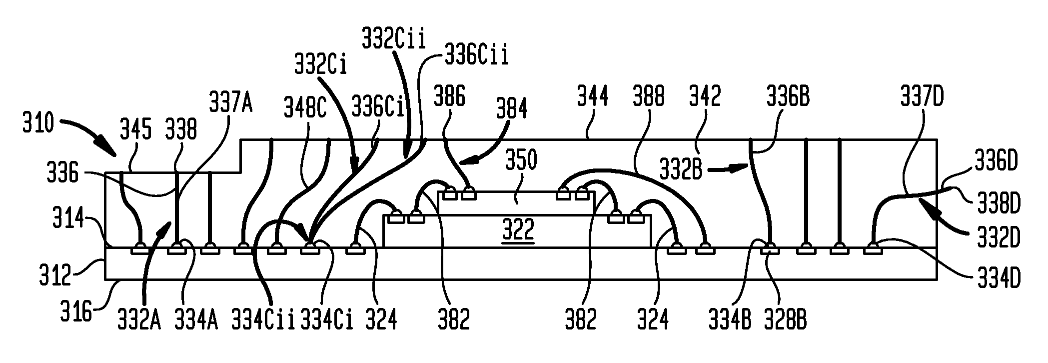
[0065]Turning now to the figures, where similar numeric references are used to indicate similar features, there is shown in FIG. 1 a microelectronic assembly 10 according to an embodiment of the present invention. The embodiment of FIG. 1 is a microelectronic assembly in the form of a packaged microelectronic element such as a semiconductor chip assembly that is used in computer or other electronic applications.

[0066]The microelectronic assembly 10 of FIG. 1 includes a substrate 12 having a first surface 14 and a second surface 16. The substrate 12 typically is in the form of a dielectric element, which is substantially flat. The dielectric element may be sheet-like and may be thin. In particular embodiments, the dielectric element can include one or more layers of organic dielectric material or composite dielectric materials, such as, without limitation: polyimide, polytetrafluoroethylene (“PTFE”), epoxy, epoxy-glass, FR-4, BT resin, thermoplastic, or thermoset plastic materials. T...


PUM


Abstract

A microelectronic assembly includes a substrate having a first surface and a second surface remote from the first surface. A microelectronic element overlies the first surface and first electrically conductive elements are exposed at one of the first surface and the second surface. Some of the first conductive elements are electrically connected to the microelectronic element. Wire bonds have bases joined to the conductive elements and end surfaces remote from the substrate and the bases, each wire bond defining an edge surface extending between the base and the end surface. An encapsulation layer extends from the first surface and fills spaces between the wire bonds such that the wire bonds are separated by the encapsulation layer. Unencapsulated portions of the wire bonds are defined by at least portions of the end surfaces of the wire bonds that are uncovered by the encapsulation layer.

Description

CROSS-REFERENCE TO RELATED APPLICATIONS[0001]This application claims the benefit of the filing date of Korean Patent Application No. 10-2011-0041843, filed May 3, 2011.TECHNICAL FIELD[0002]The subject matter of this application relates to microelectronic packages and fabrication methods thereof, particularly those which incorporate wire bonds for electrical connection with an element above a surface of an encapsulation layer.BACKGROUND OF THE INVENTION[0003]Microelectronic devices such as semiconductor chips typically require many input and output connections to other electronic components. The input and output contacts of a semiconductor chip or other comparable device are generally disposed in grid-like patterns that substantially cover a surface of the device (commonly referred to as an “area array”) or in elongated rows which may extend parallel to and adjacent each edge of the device's front surface, or in the center of the front surface. Typically, devices such as chips must b...

Claims


Application Information

Patent Timeline
IPC IPC(8): H01L23/498H01L21/56H01L21/50H01L23/48
CPCH01L23/3121H01L23/49811H01L23/5389H01L25/105H01L21/565H01L2224/16145H01L2224/16227H01L2224/48227H01L2224/4824H01L2224/48247H01L2224/73204H01L2924/19107H01L2225/06565H01L2224/48145H01L2224/73215H01L2224/45124H01L2224/32145H01L2224/32225H01L2224/32245H01L2224/73265H01L23/49517H01L23/13H01L2225/1023H01L2225/1029H01L2225/1041H01L2225/1058H01L2924/00013H01L21/4885H01L2924/1815H01L2224/16225H01L2224/13099H01L2224/13599H01L2224/05599H01L2224/05099H01L2224/29099H01L2224/29599H01L2924/00H01L2924/00012H01L2924/181H01L2224/48091H01L24/73H01L2924/00014
Inventor SATO, HIROAKIKANG, TECK-GYUHABA, BELGACEMOSBORN, PHILIP R.WANG, WEI-SHUNCHAU, ELLISMOHAMMED, ILYASMASUDA, NORIHITOSAKUMA, KAZUOHASHIMOTO, KIYOAKIINETARO, KUROSAWAKIKUCHI, TOMOYUKI
Owner TESSERA LLC
Why Eureka
Try Eureka