

Semiconductor device and method of fabricating the same
- Summary
- Abstract
- Description
- Claims
- Application Information
AI Technical Summary
Benefits of technology
Problems solved by technology
Method used
Image

Examples
experimental example
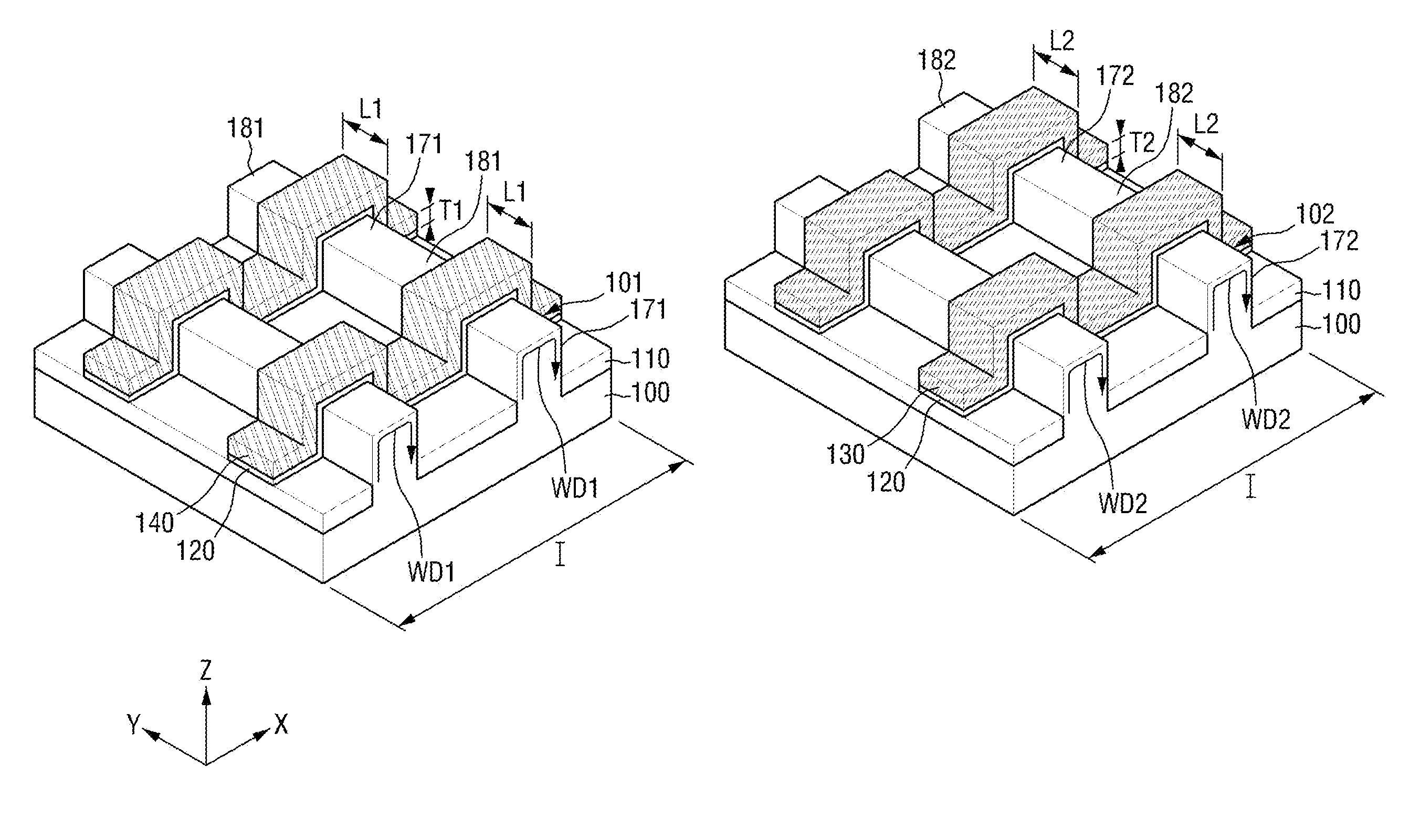
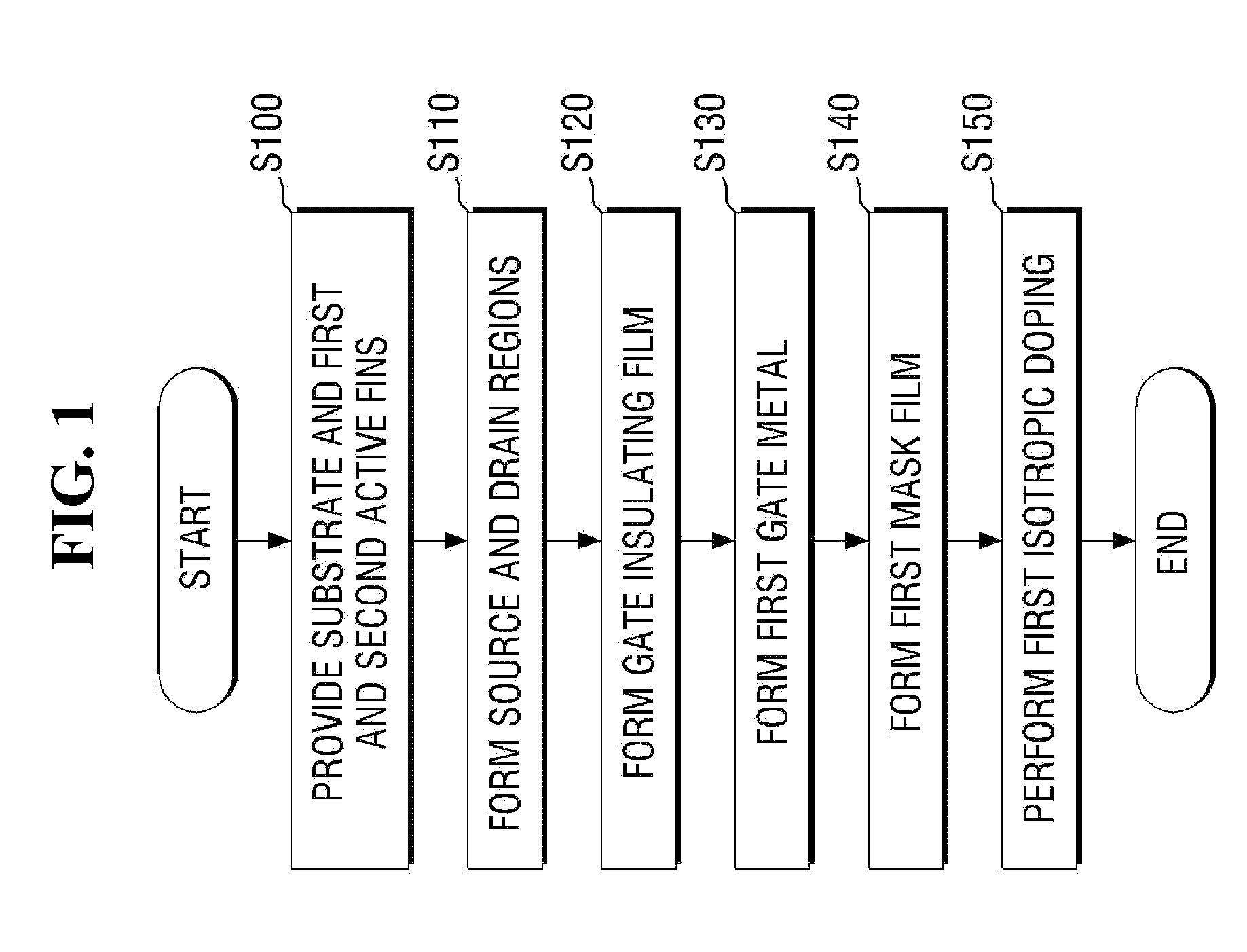
[0156]A substrate and first and second active fins which protrude at a top surface of the substrate and integrally formed on the substrate were provided, and a gate insulating film was formed on each of the first and second active fins. Then, a gate metal made of TiN was formed on the gate insulating film.
[0157]The gate insulating film formed on the second active fin was masked, and a plasma doping process was performed on the exposed gate insulating film formed on the first active fin by using argon as impurities. In this state, a C-V curve of a first transistor Q including the exposed gate insulating film formed on the first active fin and a C-V curve of a second transistor P including the masked gate insulating film formed on the second active fin were obtained. While this experimental example conforms to the embodiment described with respect to FIGS. 2-15, the results may also exemplify all the embodiments described herein (although it should be emphasized that other results are...
PUM
 Abstract
Description
Claims
Application Information