[0012]Preferred embodiments of the present invention provide a component aligning apparatus which enables a plurality of chip-type electronic components to be aligned in proper orientation even if the chip-type electronic components are made thinner, and accordingly makes it possible to apply, for example,
conductive paste to the chip-type electronic components with high precision. Also, preferred embodiments of the present invention provide an electronic component manufacturing method using the component aligning apparatus.
[0015]In another specific preferred embodiment of the component aligning apparatus according to the present invention, the component aligning apparatus further includes a feed-in jig to feed a single one of the electronic components into each of the through-holes of the guide plate, the feed-in jig being mounted on top of a stacked body in which the guide plate and the component aligning jig are stacked, the feed-in jig includes a plurality of recesses on one surface, and the recesses are arranged so as to accommodate each of the electronic components with the WL surface of each of the electronic components facing down. Accordingly, by placing the feed-in jig on top of the stacked body in which the guide plate and the component aligning jig are stacked so that the recesses of the feed-in jig face the through-holes of the guide plate, the electronic components accommodated in the recesses of the feed-in jig can be easily dropped into the through-holes and, therefore, the electronic components can be accommodated in the accommodating recesses of the component aligning jig in proper orientation more reliably.
[0017]In yet still another specific preferred embodiment of the component aligning apparatus according to the present invention, the first and second stripe-shaped spaces define a cross-shaped space in plan view. In this case, since the first and second stripe-shaped spaces are substantially orthogonal to each other, chip-type electronic components supplied in various orientations can each be accommodated in the first or second stripe-shaped space reliably and easily.
[0019]In a specific preferred embodiment of the electronic component manufacturing method according to the present invention, the electronic component manufacturing method further includes the steps of abutting an
adhesive holding member onto the WT surface on the upper side of the electronic components accommodated in the accommodating recesses of the aligning jig, transporting the electronic components while holding the electronic components by the
adhesive holding member, by moving the
adhesive holding member away from the aligning jig, and immersing the electronic components into a conductive paste from the WT surface on a side of the electronic components opposite to a side stuck on the adhesive holding member. In this case, after aligning the electronic components by the component aligning apparatus according to a preferred embodiment of the present invention, by transporting the electronic components on the adhesive holding member, and bringing the electronic components held by the adhesive holding member into contact with the conductive paste in proper orientation, the conductive paste can be applied to the electronic components with high precision from the WT surface side of the electronic components.
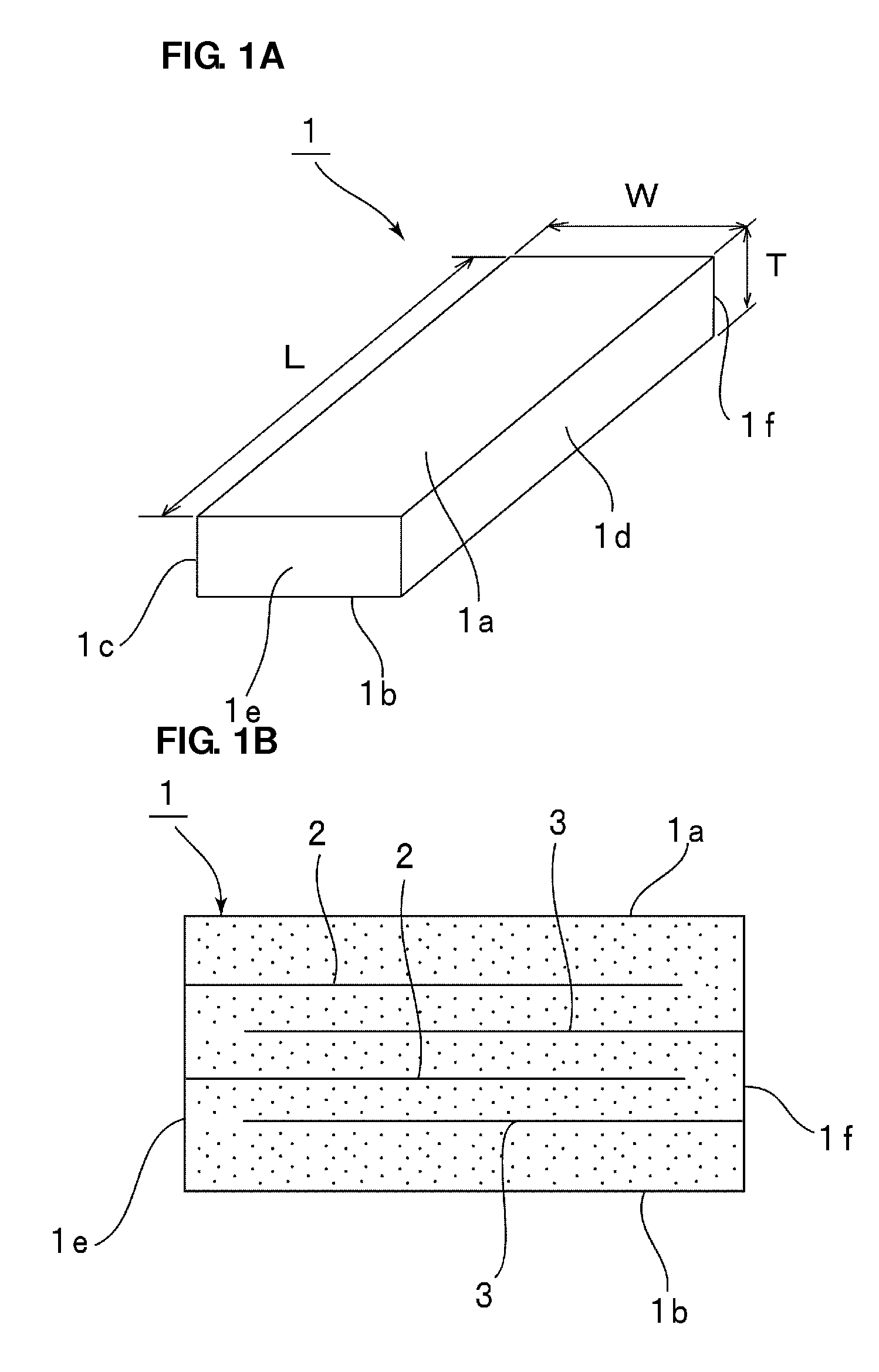
[0022]In the component aligning apparatus according to various preferred embodiments of the present invention, since the shortest separation S between the inside surfaces of each accommodating recess of the component aligning jig is set as W>S>T, the electronic components can be reliably positioned in the accommodating recesses in proper orientation, even as the electronic components are made thinner. Accordingly, by simply inserting the electronic components into the accommodating recesses of the component aligning apparatus mentioned above in accordance with the electronic component manufacturing method according to another preferred embodiment of the present invention, a plurality of electronic components can be aligned and held in a plurality of accommodating recesses reliably and properly.
[0023]Thus, for example, it becomes possible to pick up the plurality of aligned electronic components by using the adhesive holding member or the like, and perform application of conductive paste or the like with high precision and ease.

