Pin diode
a diode and pin technology, applied in the field of pin (p intrinsic n) diodes, can solve the problems of reducing the concentration of electric fields in the end part, unable to prevent the concentration of electric fields in the curved part of the anode region, and preventing so as to improve avalanche resistance, suppress the occurrence of thermal destruction, and improve the effect of avalanche resistan
- Summary
- Abstract
- Description
- Claims
- Application Information
AI Technical Summary
Benefits of technology
Problems solved by technology
Method used
Image

Examples
first embodiment
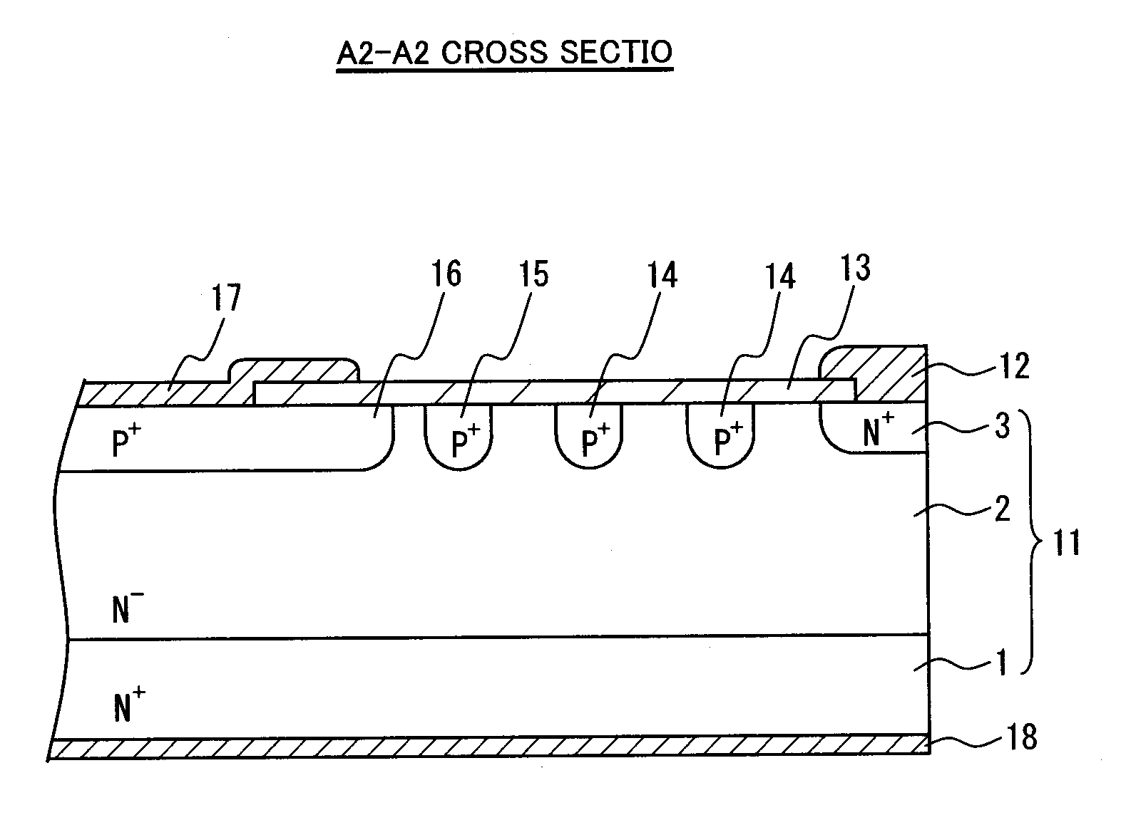
[0046]
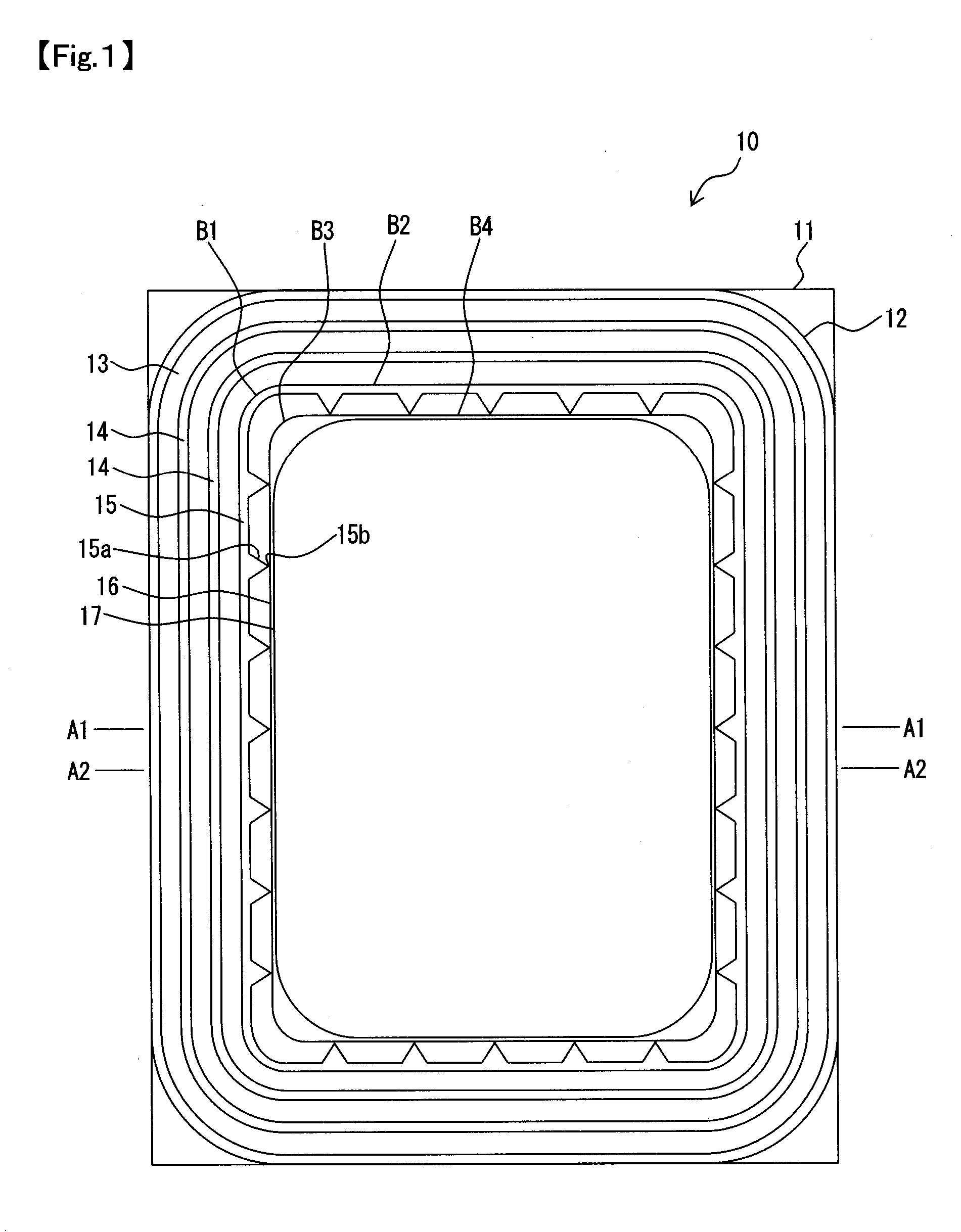
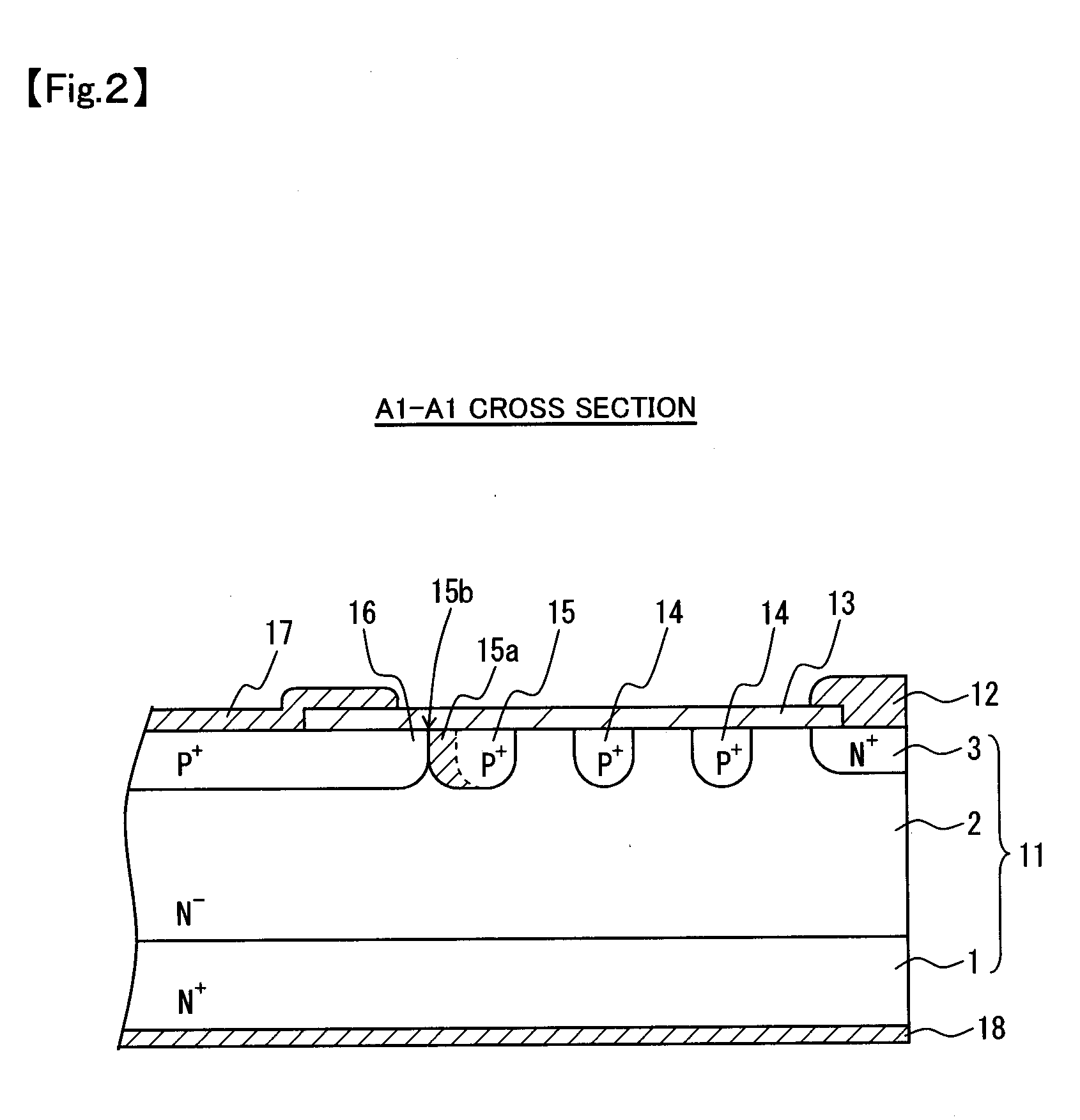
[0047]FIG. 1 is a plan view illustrating a configuration example of a PIN diode according to a first embodiment of the present invention. A PIN diode 10 is a semiconductor rectifier element including respective semiconductor layers of P-I-N, and for examples, as an FRD (Fast Recovery Diode), used for a power converter or the like.
[0048]In the PIN diode 10, on one principal surface of a semiconductor substrate 11, two FLRs 14, a separated anode region 15, a plurality of protruding parts 15a, and a main anode region 16 are formed. The main anode region 16 is an anode region including a P-type semiconductor, and on the region, a substantially rectangular shaped anode electrode 17 is formed. The main anode region 16 has a substantially rectangular outer edge of which four sides are adapted to be linear parts B4 and four vertices are adapted to be substantially arc-like curved parts B3, respectively.
[0049]The separated anode region 15 is a P-type anode region that is annularly form...
second embodiment
[0087]In the first embodiment, described is the example of the case of patterning the same shapes as those of the separated anode region 15, protruding parts 15a, and main anode region 16, which are desired to be prepared, in the same locations as those of them, and thereby accurately controlling the shape of the connecting parts 15b. On the other hand, in the present embodiment, a case of using lateral diffusion to form a protruding part 15a is described.
[0088]FIGS. 9 (a) and (b) are explanatory diagrams schematically illustrating an example of a method for manufacturing a PIN diode 10 according to the second embodiment of the present invention, in which a process of using diffusion toward lateral directions 41 to form a separated anode region 15, protruding part 15a, and main anode region 16 is illustrated. FIG. 9 (a) illustrates a shape of a mask pattern 30 at the time of forming the separated anode region 15 and main anode region 16. FIG. 9 (b) illustrates a concentration gradie...
PUM
 Abstract
Description
Claims
Application Information
 - R&D Engineer
- R&D Manager
- IP Professional
- Industry Leading Data Capabilities
- Powerful AI technology
- Patent DNA Extraction
Browse by: Latest US Patents, China's latest patents, Technical Efficacy Thesaurus, Application Domain, Technology Topic.
© 2024 PatSnap. All rights reserved.Legal|Privacy policy|Modern Slavery Act Transparency Statement|Sitemap