Cathode junction embedded p + Nano-Silicon/Crystalline Silicon/Nano-Silicon Diodes of Nano-SiC

A nano-silicon carbide and crystalline silicon technology, used in semiconductor devices, electrical components, circuits, etc., can solve problems such as irreversible damage to devices, local temperature rise of current wires, damage to electrical systems, etc.

Inactive Publication Date: 2016-08-24
扬州恒爱电子科技股份有限公司
View PDF4 Cites 0 Cited by
  • Summary
  • Abstract
  • Description
  • Claims
  • Application Information

AI Technical Summary

Problems solved by technology

This current filament will cause severe localized temperature rise, which will eventually cause irreversible damage to the device and even damage the electrical system

Method used


Image

  • Cathode junction embedded p  <sup>+</sup> Nano-Silicon/Crystalline Silicon/Nano-Silicon Diodes of Nano-SiC
  • Cathode junction embedded p  <sup>+</sup> Nano-Silicon/Crystalline Silicon/Nano-Silicon Diodes of Nano-SiC
  • Cathode junction embedded p  <sup>+</sup> Nano-Silicon/Crystalline Silicon/Nano-Silicon Diodes of Nano-SiC

Examples


Embodiment Construction

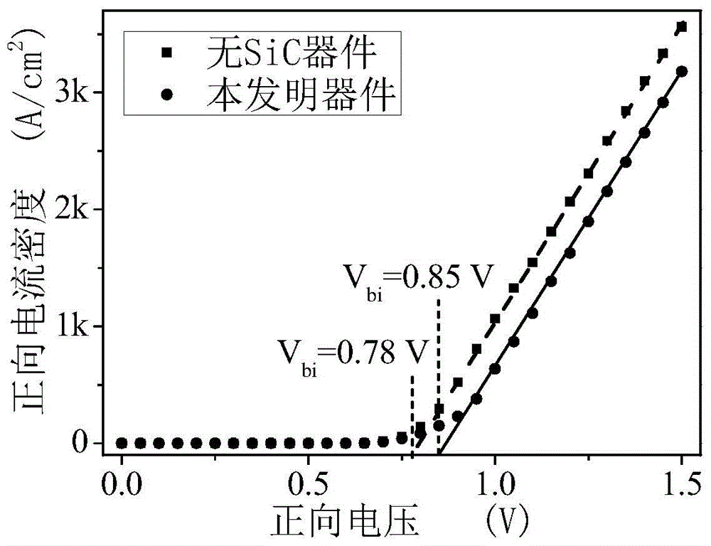
[0033] The present invention is described in detail by the following examples, which are only used to further illustrate the present invention, and cannot be interpreted as limiting the protection scope of the present invention. Technical engineers in this field can make some non-essential improvements and adjustments to the present invention according to the content of the above-mentioned invention .

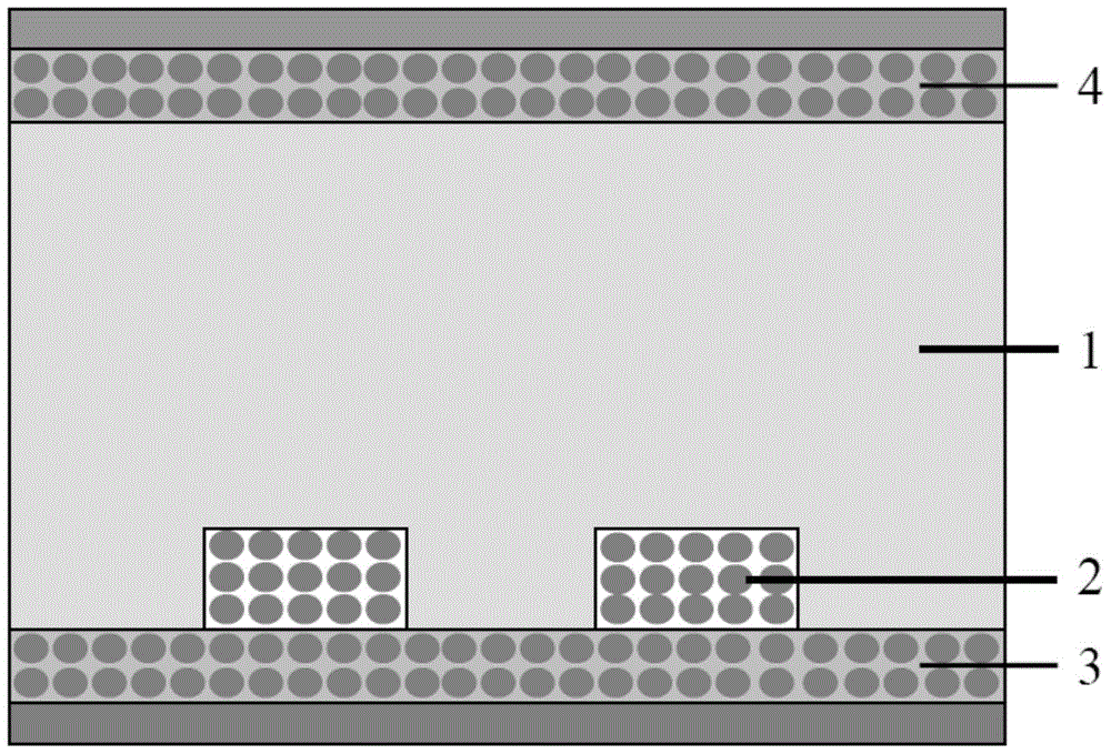
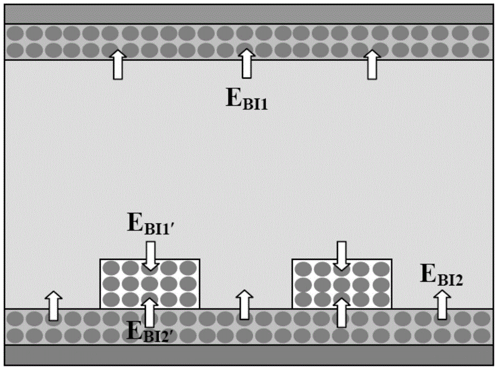
[0034] As attached to the manual figure 1 Shown, the present invention - cathode junction embedded P + Nano-silicon / crystalline silicon / nano-silicon diode of type nano-silicon carbide, its structure is: anode ohmic electrode / P + Type nano silicon layer 4 / N - Type crystalline silicon substrate 1 / N + type nano silicon layer 3 / cathode ohmic electrode,

[0035] N - Type crystalline silicon substrate 1 with N + A cathode heterojunction is formed between the nano-silicon layers 3, and the N in the cathode heterojunction - Type crystalline silicon substrate 1 side is provided w...


PUM

PropertyMeasurementUnit
thicknessaaaaaaaaaa
thicknessaaaaaaaaaa
particle sizeaaaaaaaaaa

Abstract

The invention discloses a nano silicon / crystalline silicon / nano silicon diode with P<+> type nano silicon carbide embedded a cathode junction. The nano silicon / crystalline silicon / nano silicon diode structurally comprises an anode ohmic electrode, a P<+> type nano silicon layer, an N<-> type crystalline silicon substrate, an N<+> type nano silicon layer and a cathode ohmic electrode; the cathode heterogeneous junction is formed between the N<-> type crystalline silicon substrate and the N<+> type nano silicon layer; and the P<+> type nano silicon carbide is embedded in the cathode junction. The P<+> type semiconductor is embedded into one side of the base region of the cathode junction, and therefore, reverse surge current can be suppressed, and damage to a device, caused by current filaments which are brought about by a destructive double-positive feedback dynamic avalanche effect occurring on the diode, can be avoided.

Description

technical field [0001] The invention belongs to the field of semiconductor devices, in particular to a cathode junction embedded P + Nano-silicon / crystalline silicon / nano-silicon diodes of type nano-silicon carbide. Background technique [0002] PIN structure diodes, in addition to heavily doped P + type anode area and N + In addition to the N-type cathode region, there is an I region (base region or drift region) located between the two electrodes with a relatively low doping concentration of several orders of magnitude. When the PIN type diode is forward conducting, P + and N + The type region injects a large number of holes and electrons into the I region respectively, and they form an overall electrically neutral electron-hole pair layer (plasma layer) in the I region. Due to the conductance modulation effect, the forward conduction voltage drop V of a diode with a base thickness of several hundred microns F It is also only slightly higher than the forward conducti...

Claims


Application Information

Patent Timeline
Patent Type & Authority Patents(China)
IPC IPC(8): H01L29/868H01L29/06
CPCH01L29/06H01L29/868
Inventor 韦文生
Owner 扬州恒爱电子科技股份有限公司
Why Eureka
Try Eureka