
Insulated gate bipolar transistor with improved on/off resistance

a bipolar transistor and on/off resistance technology, applied in the field of mosfet (metaloxidesemiconductor fieldeffect transistor), can solve the problems of large quantity of holes generated in semiconductor substrates, difficult to flow holes from the base region and difficult to flow holes to the front surface electrode via the contact region. , to achieve the effect of reducing contact resistance, reducing impurity concentration, and reducing impurity concentration

Active Publication Date: 2018-02-27
TOYOTA JIDOSHA KK
View PDF26 Cites 0 Cited by
  • Summary
  • Abstract
  • Description
  • Claims
  • Application Information

AI Technical Summary

Benefits of technology

The present patent provides a technology that reduces resistance and increases avalanche resistance in a MOSFET. This is achieved by forming channels in the p-type base region and the p-type first contact region in the MOSFET when it is on, and by lowering the impurity concentration of the first contact region. This allows for easier formation of channels and enables smooth flow of holes generated by the avalanche effect to the front surface electrode when the MOSFET is turned off. Overall, this technology improves the performance of MOSFETs and enhances their reliability.

Problems solved by technology

Then, the application of the high voltage to the semiconductor substrate causes a large quantity of holes to be generated in the semiconductor substrate by the avalanche effect.
Therefore, it becomes more difficult for the holes to flow from the base region to the front surface electrode via the contact region.
Further, since the hole mobility of a semiconductor substrate configured of SiC is lower than that configured of another material, it is even harder for the holes to flow to the front surface electrode via the contact region.
This makes it harder for the large quantity of holes generated by the avalanche effect to flow to the front surface electrode via the contact region, thus undesirably causing a decrease in avalanche resistance.
However, simply making the contact region larger causes the source region, which is adjacent to the contact region, to be smaller and causes an increase in resistance accordingly when the MOSFET is on.

Method used


Image

  • Insulated gate bipolar transistor with improved on/off resistance
  • Insulated gate bipolar transistor with improved on/off resistance
  • Insulated gate bipolar transistor with improved on/off resistance

Examples


Embodiment Construction

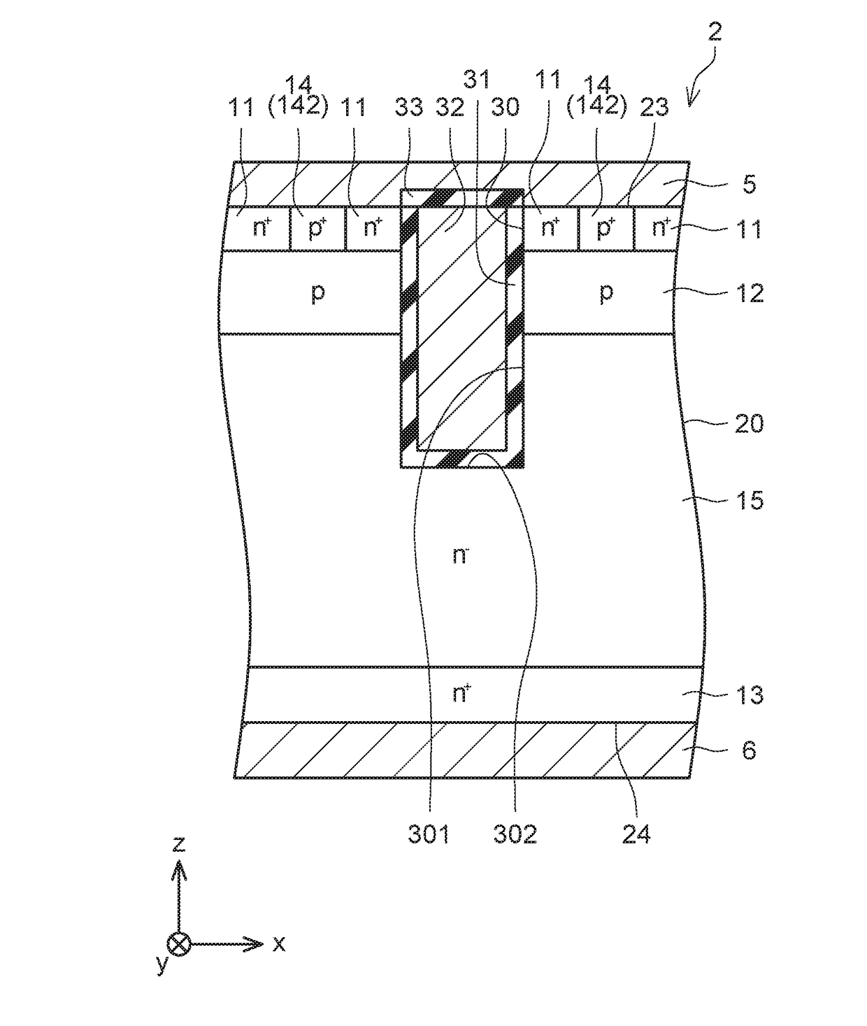
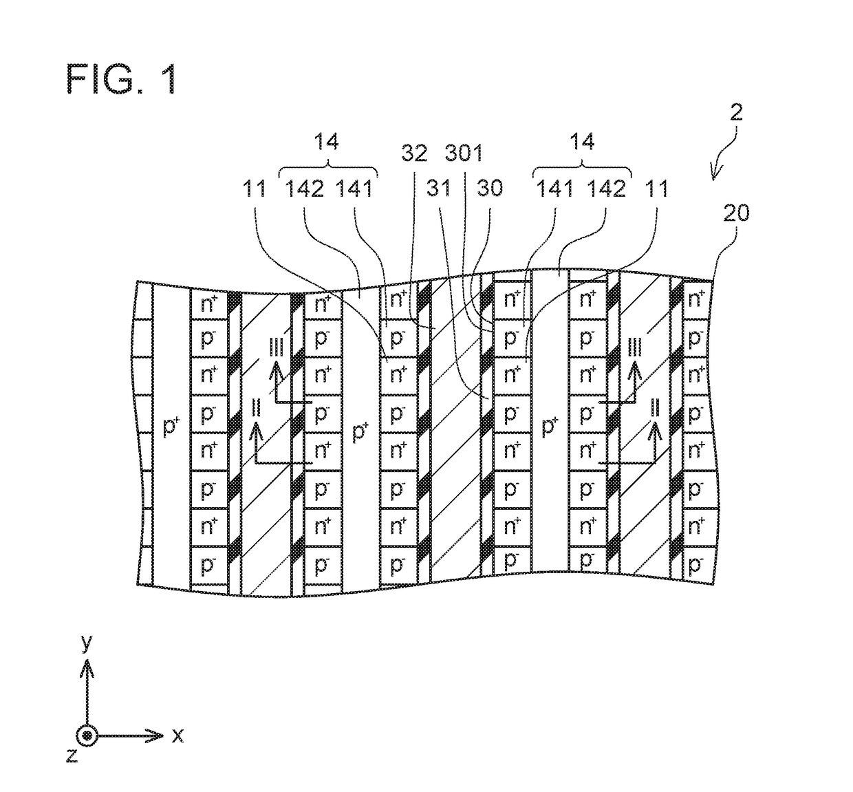
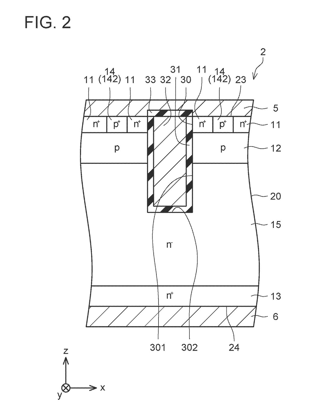
[0023]As shown in FIGS. 1 to 3, a MOSFET 2 according to an embodiment comprises a semiconductor substrate 20, a front surface electrode 5 provided on a front surface 23 of the semiconductor substrate 20, and a rear surface electrode 6 provided on a rear surface 24 of the semiconductor substrate 20. It should be noted that, for higher viewability, FIG. 1 omits to illustrate the front surface electrode 5.

[0024]The front surface electrode 5 and the rear surface electrode 6 are configured of metal such as aluminum (Al) and copper (Cu). The front surface electrode 5 covers the front surface 23 of the semiconductor substrate 20. The rear surface electrode 6 covers the rear surface 24 of the semiconductor substrate 20.

[0025]The semiconductor substrate 20 is configured of SiC (silicon carbide). The hole mobility of a semiconductor substrate configured of SiC is lower than that configured of another material. For example, a mobility of holes in a semiconductor substrate configured of SiC ran...


PUM


Abstract

In a plane view of the front surface of the semiconductor substrate, the source region and the first contact region are arranged adjacent to each other in a direction along the gate trench in an area being in contact with a side surface of the gate trench, and the second contact region is arranged adjacent to the source region and the first contact region in an area apart from the gate trench. The impurity concentration of the first contact region is lower than the impurity concentration of the second contact region.

Description

CROSS-REFERENCE TO RELATED APPLICATIONS[0001]This application claims priority to Japanese Patent Application No. 2015-060633 filed on Mar. 24, 2015, the entire contents of which are hereby incorporated by reference into the present application.TECHNICAL FIELD[0002]The present application relates to a MOSFET (metal-oxide-semiconductor field-effect transistor).DESCRIPTION OF RELATED ART[0003]Japanese Patent Application Publication No. 2005-142240 A discloses a MOSFET including: a semiconductor substrate configured of SiC; and a front surface electrode provided on a front surface of the semiconductor substrate. The semiconductor substrate includes: an n-type drift region; a p-type base region provided on a front surface side of the drift region; and a gate trench extending from the front surface of the semiconductor substrate, piercing the base region, and reaching the drift region. Further, the semiconductor substrate includes: an n-type source region provided in an area exposed on th...

Claims


Application Information

Patent Timeline
Patent Type & Authority Patents(United States)
IPC IPC(8): H01L29/78H01L29/10H01L29/16H01L29/06
CPCH01L29/7813H01L29/063H01L29/1608H01L29/1095H01L29/0696H01L29/0603H01L29/7827
Inventor SUGIMOTO, MASAHIROWATANABE, YUKIHIKOMIYAHARA, SHINICHIRO
Owner TOYOTA JIDOSHA KK
Learn More