
Graphene electronic devices having multi-layered gate insulating layer

a technology of electronic devices and gate insulating layers, applied in the direction of basic electric elements, electrical equipment, semiconductor devices, etc., can solve the problem of reducing mobility

Active Publication Date: 2012-12-13
SAMSUNG ELECTRONICS CO LTD +1
View PDF3 Cites 20 Cited by
  • Summary
  • Abstract
  • Description
  • Claims
  • Application Information

AI Technical Summary

Benefits of technology

[0014]The graphene channel layer may include single-layer graphene or bi-layer graphene. The graphene channel layer may be a nano-ribbon graphene channel layer, and the graphene electronic device may be a field effect transistor. The graphene electronic device may further include a passivation layer covering the graphene channel layer.

Problems solved by technology

However, the mobility may be reduced when graphene contacts an inorganic insulating layer such as silicon oxide or when graphene absorbs moisture.

Method used


Image

  • Graphene electronic devices having multi-layered gate insulating layer
  • Graphene electronic devices having multi-layered gate insulating layer
  • Graphene electronic devices having multi-layered gate insulating layer

Examples


Embodiment Construction

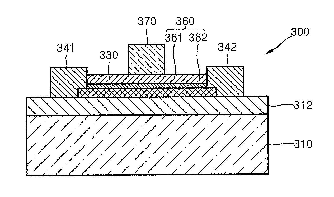
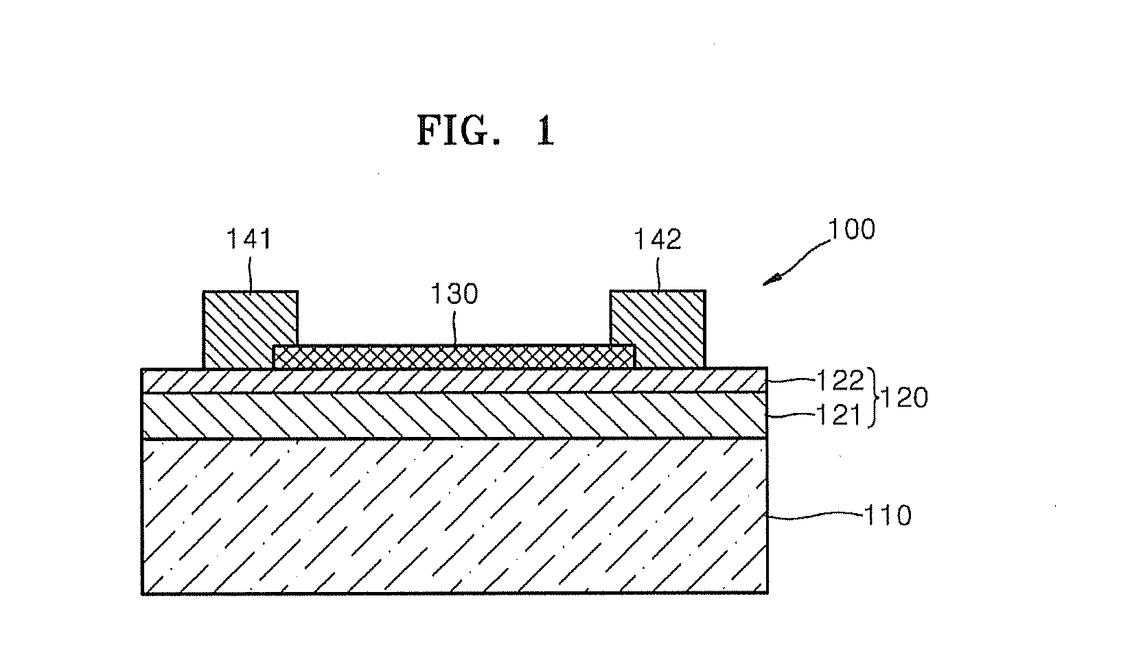
[0023]Reference will now be made in detail to embodiments, examples of which are illustrated in the accompanying drawings. In the drawings, lengths and sizes of layers and regions may be exaggerated for clarity, and also, like reference numerals refer to the like elements throughout and descriptions thereof will be omitted.

[0024]It will be understood that, although the terms first, second, third etc. may be used herein to describe various elements, these elements should not be limited by these terms. These terms are used to distinguish one element from another. Thus, a first element discussed below could be termed a second element without departing from the teachings of the present inventive concept. As used herein, the term “and / or” includes any and all combinations of one or more of the associated listed items.

[0025]The terminology used herein is for the purpose of describing particular example embodiments only and is not intended to be limiting of the present inventive concept. A...


PUM


Abstract

A graphene electronic device includes a multi-layered gate insulating layer between a graphene channel layer and a gate electrode. The multi-layered gate insulating layer includes an organic insulating layer and an inorganic insulating layer on the organic insulating layer.

Description

CROSS-REFERENCE TO RELATED APPLICATIONS[0001]This application claims the benefit of Korean Patent Application No. 10-2011-0056341, filed on Jun. 10, 2011, in the Korean Intellectual Property Office, the disclosure of which is incorporated herein in its entirety by reference.BACKGROUND[0002]1. Field[0003]Some example embodiments relate to graphene electronic devices having improved electrical characteristics by forming a multi-layered gate insulating layer between a graphene channel layer and a gate electrode.[0004]2. Description of the Related Art[0005]Graphene having a 2-dimensional hexagonal carbon structure is a new material that may replace semiconductors. Graphene is a zero gap semiconductor and has a mobility of 100,000 cm2V−1s−1 at room temperature, which is approximately 100 times higher than that of silicon. Thus, graphene may be applied to high frequency devices such as radio frequency (RF) devices.[0006]When a graphene nano-ribbon (GNR) having a graphene channel width of ...

Claims


Application Information

Patent Timeline
Patent Type & Authority Applications(United States)
IPC IPC(8): H01L29/775
CPCH01L29/1606H01L29/778H01L29/513
Inventor SONG, HYUN-JAECHO, BYUNG-JINSEO, SUN-AESHIN, WOO-CHEOL
Owner SAMSUNG ELECTRONICS CO LTD
Learn More