Graphene Nanoelectric Device Fabrication

a nano-electronic device and graphene technology, applied in the field of device fabrication, can solve the problems of difficult scaling up for commercial applications, limited technique, and lack of graphene sheets in natur

Active Publication Date: 2011-03-10
LOCKHEED MARTIN CORP
View PDF12 Cites 130 Cited by
  • Summary
  • Abstract
  • Description
  • Claims
  • Application Information

AI Technical Summary

Benefits of technology

[0008]In another exemplary embodiment, a method of forming a graphene layer is provided that includes the steps of depositing a layer of graphene or amorphous carbon at least 20 Å thick onto a substrate, and etching the carbon or graphene layer to a thickness of less than 10 Å.
[0009]In yet another exemplary embodiment, a method is provided of manufacturing a solid state electronic nanostructure including a graphene layer segment. According to this method, a graphene layer segment is deposited onto a substrate and a protective sacrificial layer is deposited over the graphene layer segment. An electronically insulating layer is deposited over the protective sacrificial layer and one or more openings are etched into the insulator layer. The protective sacrificial layer is then removed to form a cavity between the graphene layer and the insulator layer, thus passivating the graphene layer. An electrically conductive material may then be deposited into the one or more openings in the insulato...

Problems solved by technology

Graphene sheets do not readily exist in nature, with graphite being made up of large numbers of graphene sheets layered one on top of another.
However, while a substantial body of literature exists on the manufacture of carbon nanotubes, experiments for the manufacture of graphene sheets on a nanoscopic or atomic layer scale have generally been conducted using techniques that would be difficult to scale up for commercial application.
This technique may be limited because graphene may not be deposited over an entire wafer, and certain coating techniques may produce relatively thick coatings with multiple layers of graphene.
Another technique involves thermal decomposition of silicon carbide (SiC) for forming graphene; however, this technique also may not deposit graphene over an entire wafer, and although the thermal decomposition of SiC may be performed with complementary m...

Method used


Image

  • Graphene Nanoelectric Device Fabrication
  • Graphene Nanoelectric Device Fabrication
  • Graphene Nanoelectric Device Fabrication

Examples


Embodiment Construction

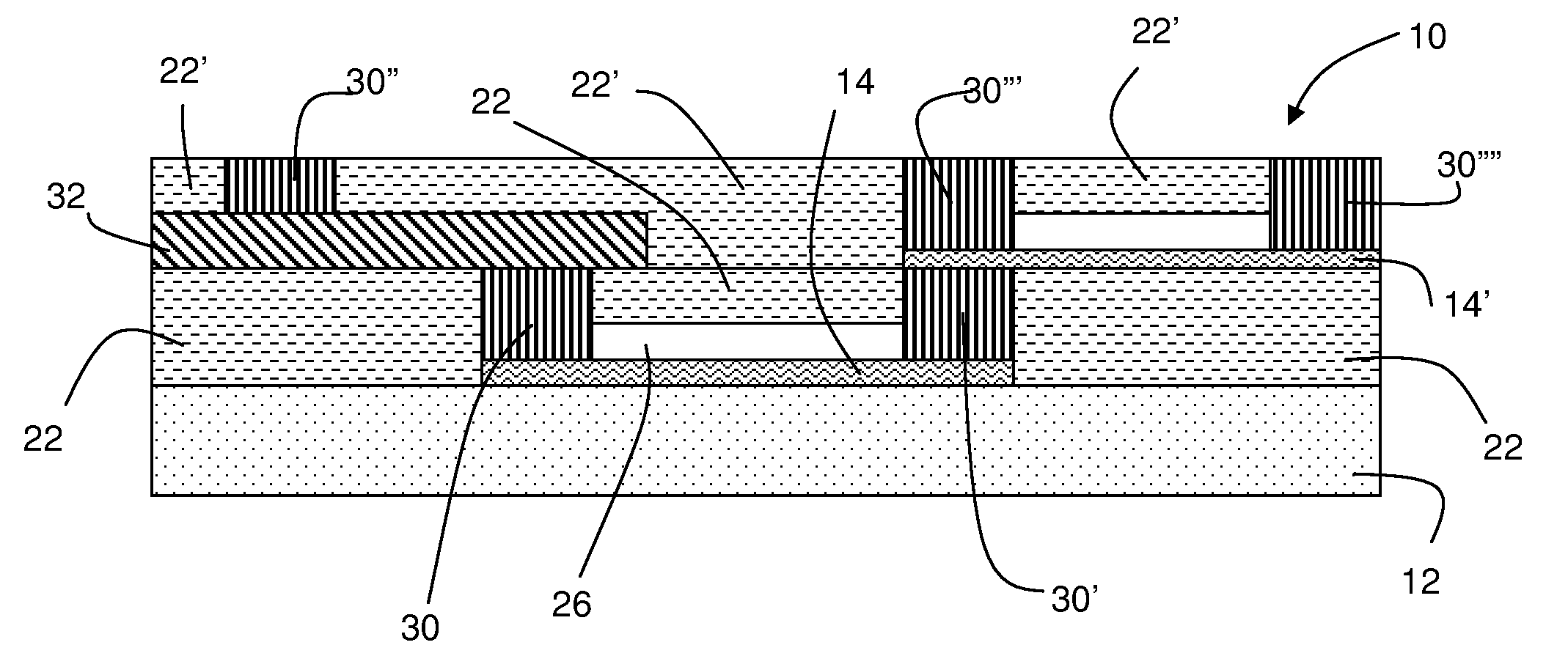
[0021]In one exemplary embodiment, a dispersion of functionalized graphene in a solvent is prepared and applied as a coating onto a substrate. Exemplary substrates include silicon, thermal oxide, silicon oxide, aluminum oxide, hafnium oxide, silicon nitride, tungsten, tungsten / titanium, aluminum, copper, and other known insulators, semiconductors, or metallic surfaces. Functionalized graphene may be prepared by starting with manufactured graphene fragments. Such graphene fragments are typically prepared by mechanical exfoliation of graphite, and are commercially available. Other techniques may also be used such as opening of carbon nanotubes to form graphene nanoribbons (e.g., in a solution of potassium permanganate and sulfuric acid or by plasma etching of CNT's partially embedded in a polymeric film followed by dissolution of the polymeric film). Another technique to form a graphene based solution is to oxidize High Ordered Pyrolitic Graphite (HOPG) or graphite, which is a known p...


PUM


Abstract

Embodiments of the present invention provide methods for fabricating graphene nanoelectronic devices with semiconductor compatible processes, which allow wafer scale fabrication of graphene nanoelectronic devices. Embodiments of the present invention also provide methods for passivating graphene nanoelectronic devices, which enable stacking of multiple graphene devices and the creation of high density graphene based circuits. Other embodiments provide methods for producing devices with graphene layer segments having multiple thicknesses.

Description

CROSS-REFERENCES TO RELATED APPLICATIONS[0001]This patent application claims priority to U.S. Provisional Patent Application Ser. Nos. 61 / 241,359 filed Sep. 10, 2009 and 61 / 326,561 filed Apr. 21, 1010, the disclosures of which are incorporated herein by reference in their entirety.BACKGROUND OF THE INVENTION[0002]The present invention relates generally to device fabrication, and more particularly to graphene nanoelectronic device fabrication.[0003]Graphene is a crystalline structure of sp2-hybridized carbon bonded together in a honeycomb-like sheet lattice of six-membered rings. Graphene sheets do not readily exist in nature, with graphite being made up of large numbers of graphene sheets layered one on top of another. An individual graphene sheet has a thickness of a single atom, but graphene has only recently been produced or isolated in thicknesses approaching a single sheet. A carbon nanotube may be conceptualized as a nanoscopic segment of a graphene sheet that has been rolled ...

Claims


Application Information

Patent Timeline
IPC IPC(8): H01L21/20
CPCB82Y30/00H01L21/31127C01B31/043C01B31/0446C01B31/0476C01B31/0484C01B2204/02C01B2204/04C01B2204/22H01L21/02491H01L21/02527H01L21/0262H01L21/02628H01L29/1606H01L21/02282B82Y40/00C01B32/23C01B32/184C01B32/192C01B32/194
Inventor WARD, JONATHAN W.O'CONNOR, MICHAEL J.
Owner LOCKHEED MARTIN CORP
Why Eureka
Try Eureka