Methods of filling trenches using high-density plasma deposition (HDP)

a plasma deposition and trench technology, applied in the field of fabricating integrated circuit devices, can solve the problems of reducing the width of the trench, difficult to fill the narrow trench, and discontinuities,

Active Publication Date: 2005-02-17
SAMSUNG ELECTRONICS CO LTD
View PDF3 Cites 347 Cited by
  • Summary
  • Abstract
  • Description
  • Claims
  • Application Information

AI Technical Summary

Problems solved by technology

However, as circuit densities continue to increase, the widths of the trenches continue to decrease.
As a result, it may become increasingly difficult to fill the narrow trenches, which may lead to unwanted voids and discontinuities in the insulating regions.
However, as illustrated in FIG. 3B, filling higher gap aspect ratios may result in voids 410 due to cusps 420 prematurely closing the gap / trench even if the etch / dep ratio is optimized to 1 at the element corners.
If the etch rate is increased to keep the gaps open longer, undesirable corner clipping can occur.

Method used


Image

  • Methods of filling trenches using high-density plasma deposition (HDP)
  • Methods of filling trenches using high-density plasma deposition (HDP)
  • Methods of filling trenches using high-density plasma deposition (HDP)

Examples


Embodiment Construction

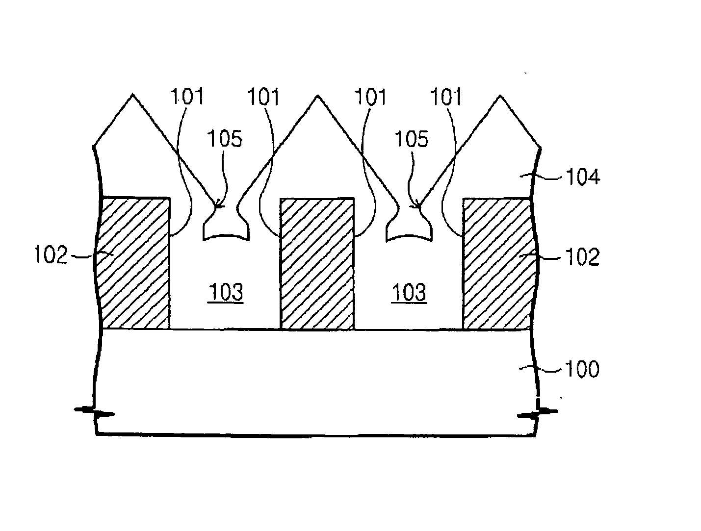
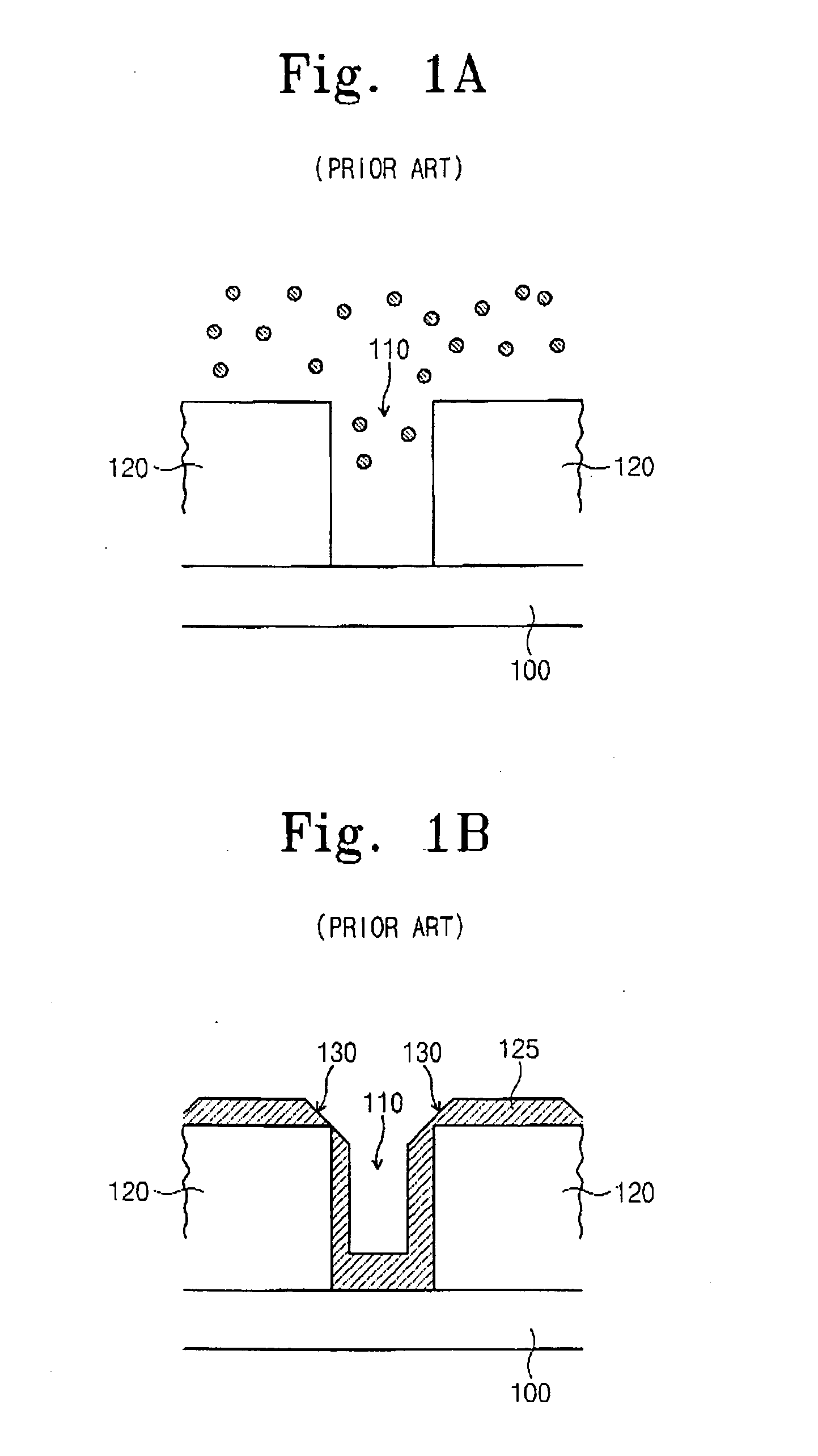
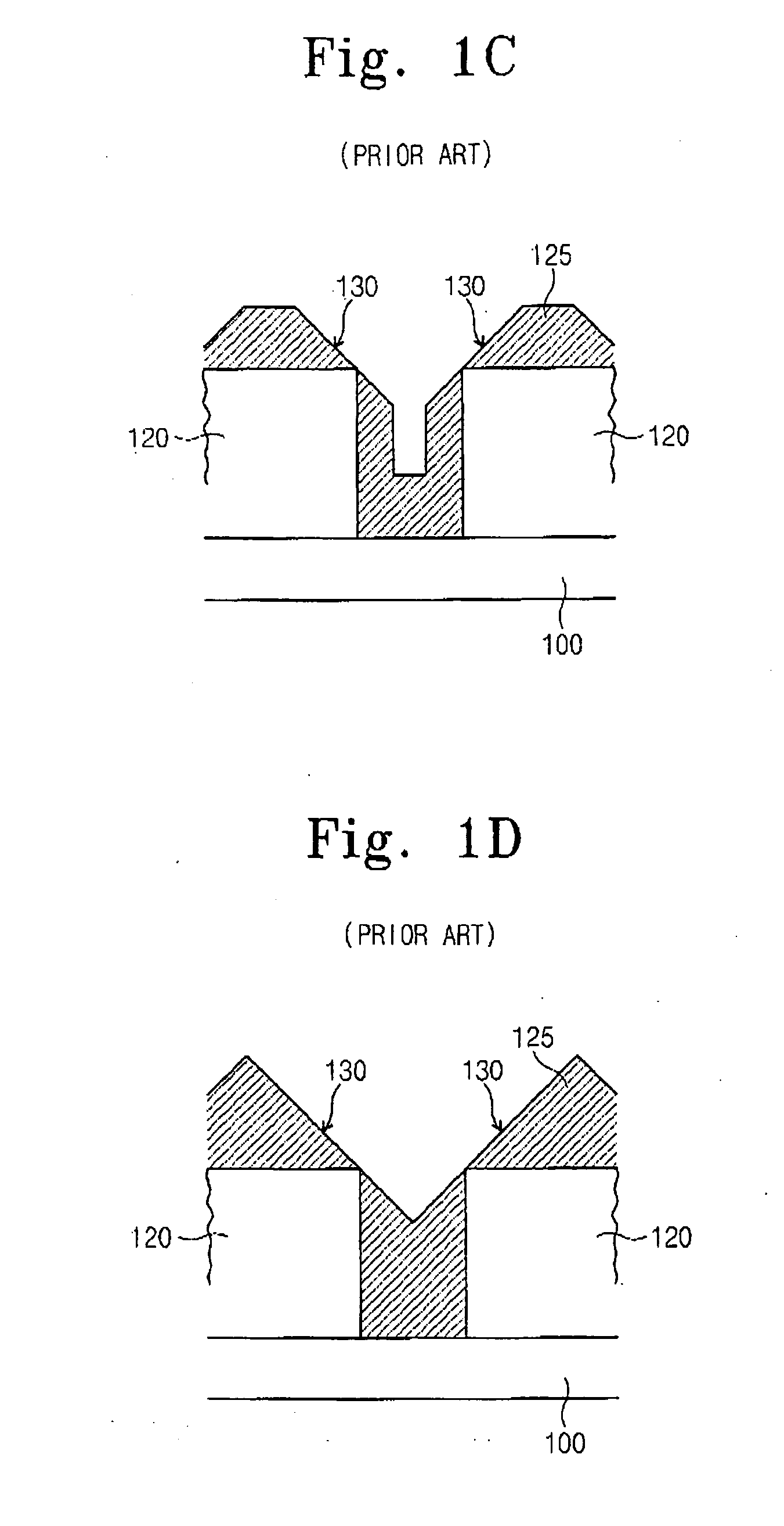
[0029] The invention now will be described more fully hereinafter with reference to the accompanying drawings, in which embodiments of the invention are shown. This invention may, however, be embodied in many different forms and should not be construed as limited to the embodiments set forth herein. Rather, these embodiments are provided so that this disclosure will be thorough and complete, and will fully convey the scope of the invention to those skilled in the art. In the drawings, the size and relative sizes of layers and regions may be exaggerated for clarity. Like numbers refer to like elements throughout.

[0030] It will be understood that when an element such as a layer, region or substrate is referred to as being “on” another element, it can be directly on the other element or intervening elements may also be present. The term“directly on” means that there are no intervening elements. It will be understood that, although the terms first, second, etc. may be used herein to de...


PUM

PropertyMeasurementUnit
temperatureaaaaaaaaaa
bias poweraaaaaaaaaa

Abstract

Methods of filling trenches / gaps defined by circuit elements on an integrated circuit substrate are provided. The methods include forming a first high-density plasma layer on an integrated circuit substrate including at least one trench thereon using a first reaction gas. The first high-density plasma layer is etched using an etch gas including nitrogen fluoride gas (NF3). A second high-density plasma layer is formed on the etched first high-density plasma layer using a second reaction gas including nitrogen fluoride.

Description

CLAIM OF PRIORITY [0001] This application is related to and claims priority from Korean Patent Application No. 10-2003-56637, filed on Aug. 14, 2003, the disclosure of which is hereby incorporated herein by reference as if set forth in its entirety. FIELD OF THE INVENTION [0002] The present invention relates to methods of fabricating integrated circuit devices and, more particularly, methods for filling trenches on integrated circuit substrates in integrated circuit devices. BACKGROUND OF THE INVENTION [0003] As integrated circuit technology advances, circuit elements and interconnections on substrates have become increasingly more dense. In order to reduce the likelihood of unwanted interactions between the circuit elements on the integrated circuit substrate, insulating regions are provided in trenches / gaps located on the integrated circuit substrates to physically and / or electrically isolate the circuit elements and conductive lines associated therewith. However, as circuit densi...

Claims


Application Information

Patent Timeline
Patent Type & Authority Applications(United States)
IPC IPC(8): H01L21/762C23C14/32H01L21/768
CPCC23C16/045H01L21/02164H01L21/76837H01L21/31612H01L21/76227H01L21/02274C23C14/32
Inventor CHA, YONG-WONNA, KYU-TAE
Owner SAMSUNG ELECTRONICS CO LTD
Why Eureka
Try Eureka