Methods of atomic layer deposition of hafnium oxide / erbium oxide bi-layer as advanced gate dielectrics

a technology of advanced gate dielectrics and atomic layer deposition, which is applied in the field of forming date dielectrics and devices, can solve the problems of reducing the performance of the device, reducing the efficiency of the device, and difficulty in maintaining the dielectric property below about 2 nm thickness, so as to achieve fewer defects and improve the effect of electrical properties

Inactive Publication Date: 2013-11-28
INTERMOLECULAR
View PDF6 Cites 342 Cited by
  • Summary
  • Abstract
  • Description
  • Claims
  • Application Information

AI Technical Summary

Benefits of technology

[0010]In some embodiments, provided is a gate dielectric, and a semiconductor device utilizing the gate dielectric, including a bi-layer of hafnium oxide on erbium oxide. Bi-layer of hafnium oxide on erbium oxide can have fewer defects, offering improved electrical properties, suitable for high k gate dielectrics in semiconductor device applications.

Problems solved by technology

When SiO2 is used as the gate dielectric, it is difficult to maintain its dielectric property below about 2 nm thickness due to the high tunneling leakage.
The fabrication of high-k gate dielectric layers can provide difficulty in realizing the full benefits of the high dielectric constant.
The traps can degrade the device performance, such as sub-threshold slope, threshold voltage, flatband voltage shift, and Frenkel-Poole tunneling leakage.

Method used


Image

  • Methods of atomic layer deposition of hafnium oxide / erbium oxide bi-layer as advanced gate dielectrics
  • Methods of atomic layer deposition of hafnium oxide / erbium oxide bi-layer as advanced gate dielectrics
  • Methods of atomic layer deposition of hafnium oxide / erbium oxide bi-layer as advanced gate dielectrics

Examples


Embodiment Construction

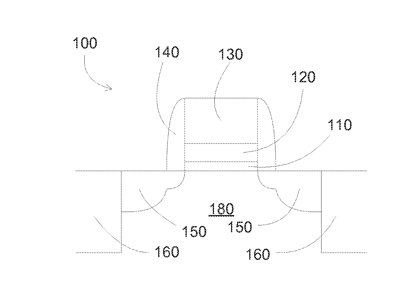
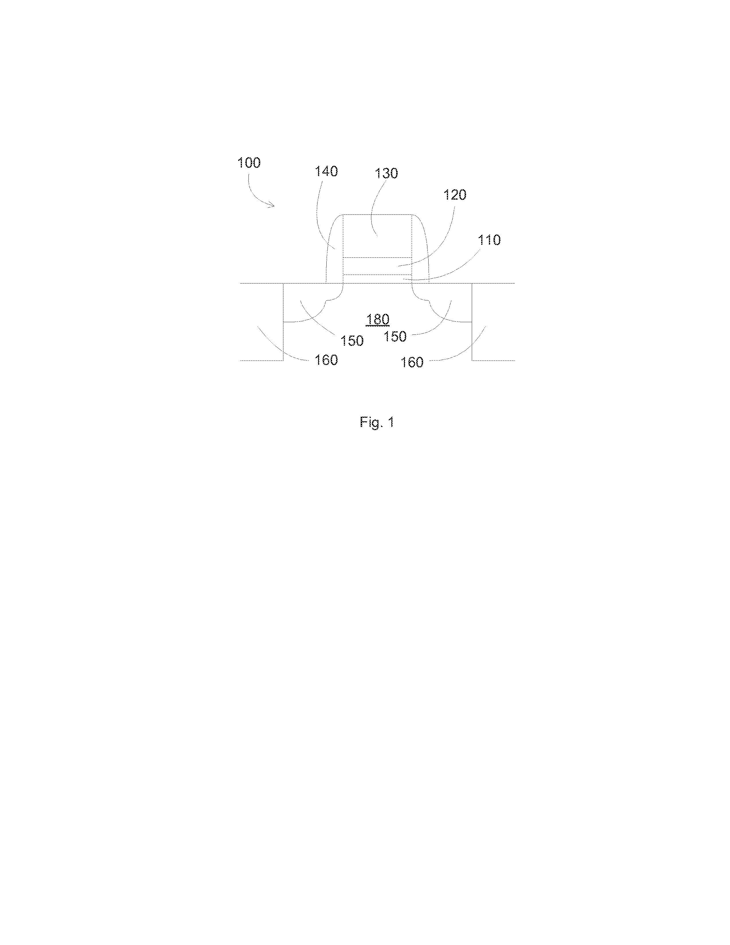
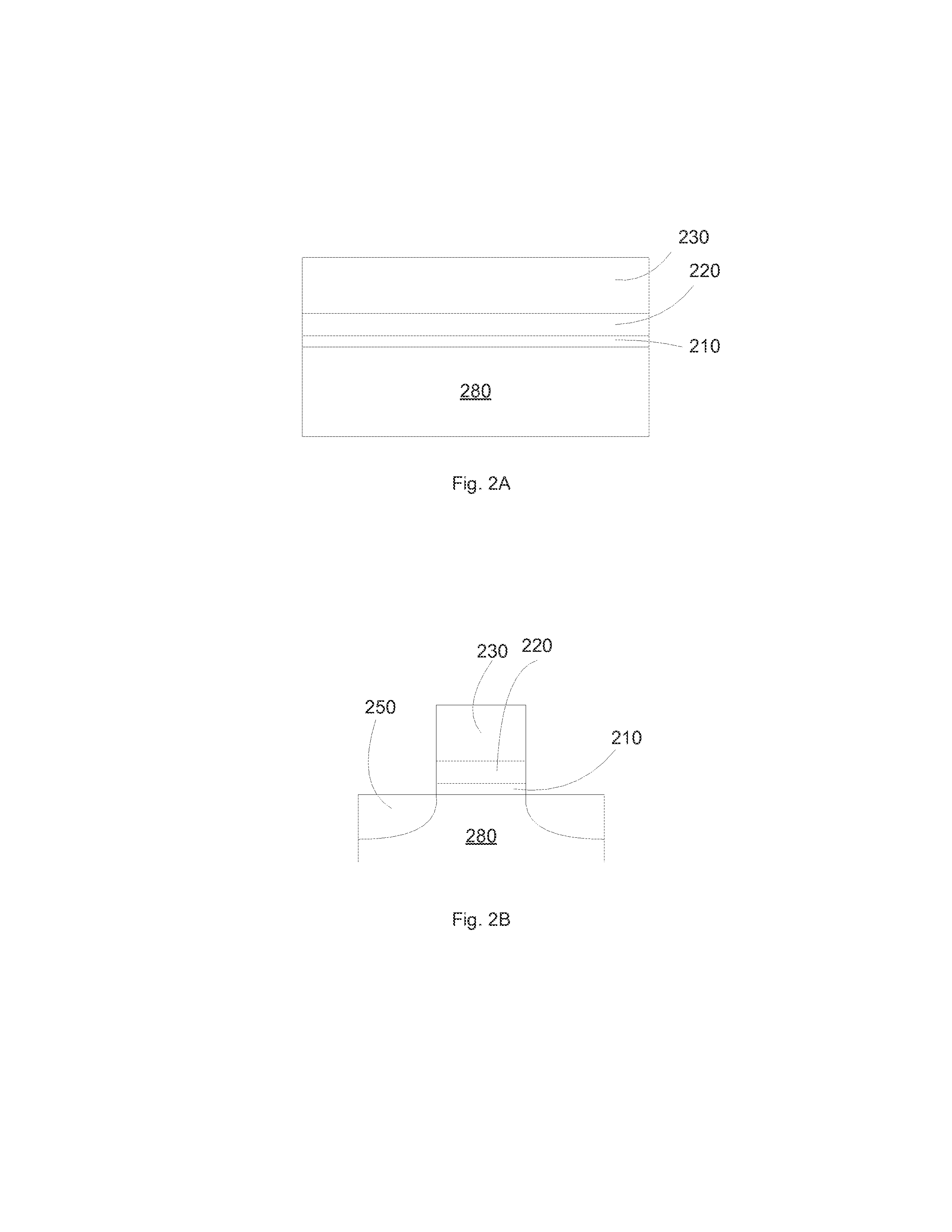
[0020]A detailed description of one or more embodiments is provided below along with accompanying figures. The detailed description is provided in connection with such embodiments, but is not limited to any particular example. The scope is limited only by the claims and numerous alternatives, modifications, and equivalents are encompassed. Numerous specific details are set forth in the following description in order to provide a thorough understanding. These details are provided for the purpose of example and the described techniques may be practiced according to the claims without some or all of these specific details. For the purpose of clarity, technical material that is known in the technical fields related to the embodiments has not been described in detail to avoid unnecessarily obscuring the description.

[0021]In some embodiments, methods, and structures fabricated from the methods, to form a hafnium oxide gate dielectric are provided. The present hafnium oxide gate dielectric...


PUM

PropertyMeasurementUnit
thicknessaaaaaaaaaa
thicknessaaaaaaaaaa
equivalent oxide thicknessaaaaaaaaaa

Abstract

Provided is a two-step ALD deposition process for forming a gate dielectric involving an erbium oxide layer deposition followed by a hafnium oxide layer deposition. Hafnium oxide can provide a high dielectric constant, high density, large bandgap and good thermal stability. Erbium oxide can act as a barrier against oxygen diffusion, which can lead to increasing an effective oxide thickness of the gate dielectric and preventing hafnium-silicon reactions that may lead to higher leakage current.

Description

FIELD OF THE INVENTION[0001]This invention relates generally to semiconductor devices and, more particularly, to methods for forming date dielectrics and devices formed using these methods.BACKGROUND OF THE INVENTION[0002]As integrated circuit feature sizes decrease, other device dimensions also need to scale down to maintain the proper device operation. For example, as gate conductor widths are being reduced, the thickness of the gate dielectric needs to decrease to provide proper capacitance to control the transistor.[0003]To meet the requirements of sub-100 nm devices, an equivalent oxide thickness (EOT) of less than 1.5 nm is needed. When SiO2 is used as the gate dielectric, it is difficult to maintain its dielectric property below about 2 nm thickness due to the high tunneling leakage.[0004]High-k materials, i.e., dielectric materials having a higher dielectric constant (k) than that of SiO2 (k ˜3.9), can provide a high capacitance with higher thickness, and thus have been stud...

Claims


Application Information

Patent Timeline
Patent Type & Authority Applications(United States)
IPC IPC(8): H01L21/316H01L29/78
CPCH01L29/78H01L21/02181H01L21/02192H01L21/022H01L21/0228C23C16/405C23C16/45529C23C16/45553H01L21/28194H01L29/4966H01L29/517H01L29/512
Inventor TONG, JINHONG
Owner INTERMOLECULAR
Why Eureka
Try Eureka