Densification for flowable films

a flowable film and density technology, applied in the direction of electric discharge tubes, coatings, chemical vapor deposition coatings, etc., can solve the problems of dielectric material, dielectric material, dielectric material, structural features of the device having decreased spatial dimensions, etc., to increase the etch tolerance of the processed layer

Inactive Publication Date: 2013-10-31
APPLIED MATERIALS INC
View PDF8 Cites 353 Cited by
  • Summary
  • Abstract
  • Description
  • Claims
  • Application Information

AI Technical Summary

Benefits of technology

[0007]A method of forming a dielectric layer is described. The method first deposits an initially-flowable layer on a substrate. The dielectric layer is flowable during the operation of forming the dielectric layer. The initially-flowable layer is then densified by exposing

Problems solved by technology

The decreasing feature sizes result in structural features on the device having decreased spatial dimensions.
The widths of gaps and trenches on the device narrow to a point where the aspect ratio of gap depth to its width becomes high enough to make it challenging to fill the gap with dielectric material.
The depositing dielectric material is prone to clog at the top before the gap completely fills, producing a void or seam in the middle of the gap.
However, once these highly flowable materials are deposited, they have to be hardened into a solid dielectric materia

Method used


Image

  • Densification for flowable films
  • Densification for flowable films
  • Densification for flowable films

Examples


Embodiment Construction

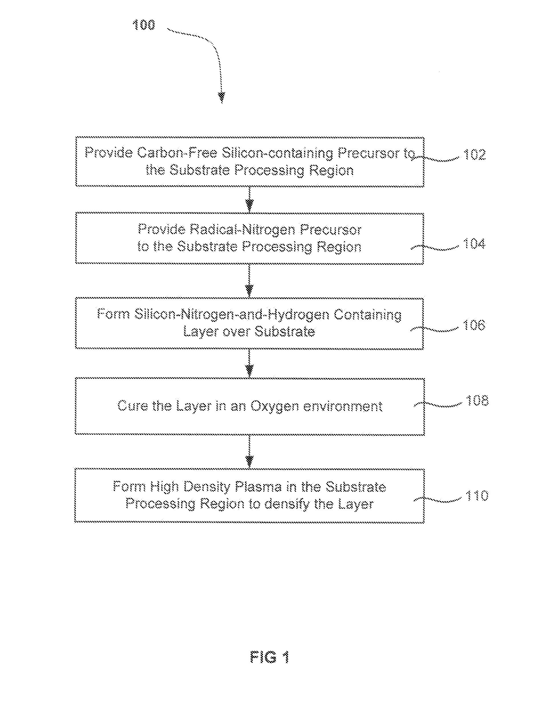
[0017]A method of forming a dielectric layer is described. The method first deposits an initially-flowable layer on a substrate. The initially-flowable layer is then densified by exposing the substrate to a high-density plasma (HDP). Essentially no additional material is deposited on the initially-flowable layer, in embodiments, but the impact of the accelerated ionic species serves to condense the layer and increase the etch tolerance of the processed layer.

[0018]Post-processing an initially-flowable dielectric layer with a high density plasma has been found to dramatically densify and reduce the wet etch rate of the processed dielectric layer. The flowable layer may be deposited by a process such as spin-on glass (SOG) spin-on dielectric (SOD), an eHARP process (H2O-TEOS-O3), SACVD or a flowable CVD process such as radical-component CVD. Flowable films can have a reduced density and elevated etch rate compared to non-flowable films. The high density plasma treatments described her...


PUM

PropertyMeasurementUnit
Temperatureaaaaaaaaaa
Poweraaaaaaaaaa
Thicknessaaaaaaaaaa

Abstract

A method of forming a dielectric layer is described. The method first deposits an initially-flowable layer on a substrate. The initially-flowable layer is then densified by exposing the substrate to a high-density plasma (HDP). Essentially no additional material is deposited on the initially-flowable layer, in embodiments, but the impact of the accelerated ionic species serves to condense the layer and increase the etch tolerance of the processed layer.

Description

CROSS-REFERENCES TO RELATED APPLICATIONS[0001]This application claims the benefit of U.S. Provisional Application No. 61 / 640,514, filed Apr. 30, 2012, and titled “IMPROVED DENSIFICATION FOR FLOWABLE FILMS,” which is hereby incorporated herein in its entirety for all purposes.BACKGROUND OF THE INVENTION[0002]Semiconductor device geometries have dramatically decreased in size since their introduction several decades ago. Modern semiconductor fabrication equipment routinely produce devices with 32 nm, 28 nm and 22 nm feature sizes, and new equipment is being developed and implemented to make devices with even smaller geometries. The decreasing feature sizes result in structural features on the device having decreased spatial dimensions. The widths of gaps and trenches on the device narrow to a point where the aspect ratio of gap depth to its width becomes high enough to make it challenging to fill the gap with dielectric material. The depositing dielectric material is prone to clog at ...

Claims


Application Information

Patent Timeline
IPC IPC(8): H01L21/02
CPCH01L21/02271H01L21/02282H01J37/321C23C16/56H01L21/02164H01L21/0217H01L21/02219H01L21/02274H01L21/02326H01L21/02337H01L21/0234H01L21/31H10B12/00
Inventor LIANG, JINGMEIHONG, SUKWONCHOI, JUN TAE
Owner APPLIED MATERIALS INC
Why Eureka
Try Eureka