Doping of dielectric layers

a technology of dielectric layers and dielectric layers, which is applied in the direction of basic electric elements, semiconductor/solid-state device manufacturing, electric apparatus, etc., can solve the problems achieve the effects of reducing the evolution of film properties, preventing shrinkage, and increasing etch toleran

Inactive Publication Date: 2013-08-22
APPLIED MATERIALS INC
View PDF25 Cites 535 Cited by
  • Summary
  • Abstract
  • Description
  • Claims
  • Application Information

AI Technical Summary

Benefits of technology

[0005]Methods are described for forming and treating a flowable silicon-carbon-and-nitrogen-containing layer on a semiconductor substrate. The silicon and carbon constituents may come from a silicon-and-carbon-containing precursor while the nitrogen may come from a nitrogen-containing precursor that has been activated to speed the reaction of the nitrogen with the silicon-and-carbon-containing precursor at lower deposition temperatures. The initially-flowable silicon-carbon-and-nitrogen-containing layer is ion implanted to increase etch tolerance, prevent shrinkage, adjust film tension and / or adjust electrical characteristics. Ion implantation may also remove components which enabled the flowability, but are no longer needed after deposition. Some treatments using ion implantation have been found to decrease the evolution of properties of the film upon exposure to atmosphere.

Problems solved by technology

Some treatments using ion implantation have been found to decrease the evolution of properties of the film upon exposure to atmosphere.

Method used


Image

  • Doping of dielectric layers
  • Doping of dielectric layers
  • Doping of dielectric layers

Examples


Embodiment Construction

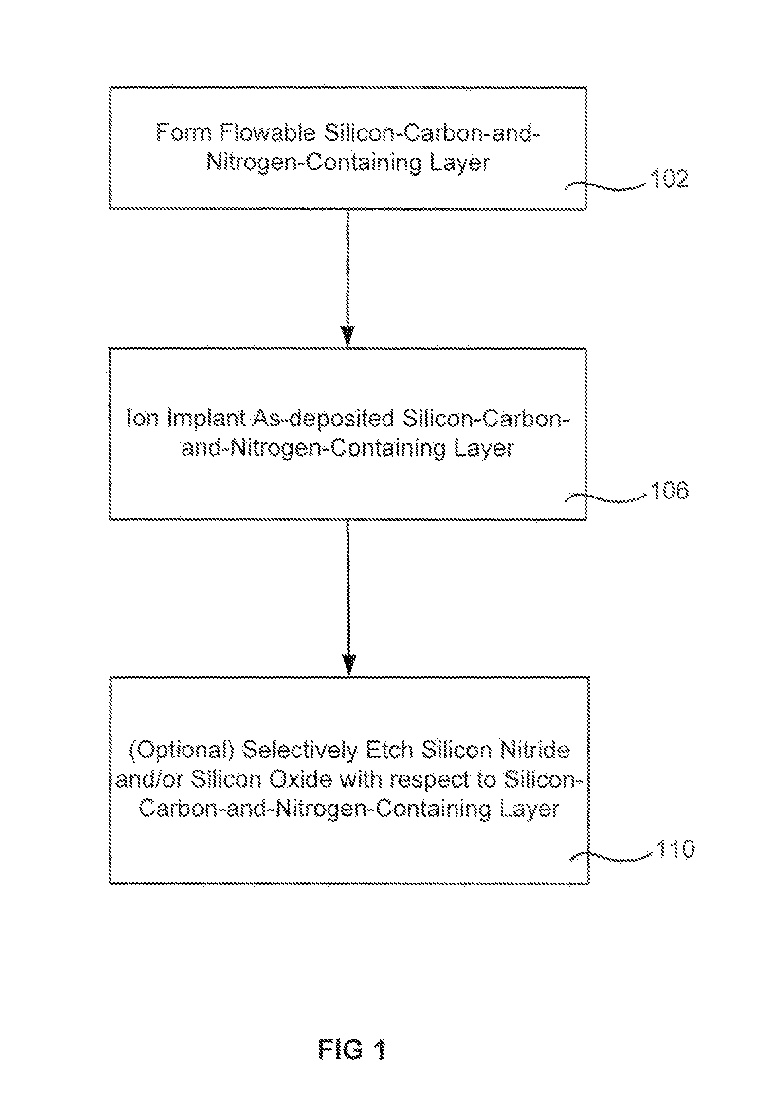
[0013]Methods are described for forming and treating a flowable silicon-carbon-and-nitrogen-containing layer on a semiconductor substrate. The silicon and carbon constituents may come from a silicon-and-carbon-containing precursor while the nitrogen may come from a nitrogen-containing precursor that has been activated to speed the reaction of the nitrogen with the silicon-and-carbon-containing precursor at lower deposition temperatures. The initially-flowable silicon-carbon-and-nitrogen-containing layer is ion implanted to increase etch tolerance, prevent shrinkage, adjust film tension and / or adjust electrical characteristics. Ion implantation may also remove components which enabled the flowability, but are no longer needed after deposition. Some treatments using ion implantation have been found to decrease the evolution of properties of the film upon exposure to atmosphere.

[0014]The initial deposition of the flowable as-deposited silicon-carbon-and-nitrogen-containing layer may ex...


PUM

PropertyMeasurementUnit
temperatureaaaaaaaaaa
total poweraaaaaaaaaa
feature sizesaaaaaaaaaa

Abstract

Methods are described for forming and treating a flowable silicon-carbon-and-nitrogen-containing layer on a semiconductor substrate. The silicon and carbon constituents may come from a silicon-and-carbon-containing precursor while the nitrogen may come from a nitrogen-containing precursor that has been activated to speed the reaction of the nitrogen with the silicon-and-carbon-containing precursor at lower deposition temperatures. The initially-flowable silicon-carbon-and-nitrogen-containing layer is ion implanted to increase etch tolerance, prevent shrinkage, adjust film tension and/or adjust electrical characteristics. Ion implantation may also remove components which enabled the flowability, but are no longer needed after deposition. Some treatments using ion implantation have been found to decrease the evolution of properties of the film upon exposure to atmosphere.

Description

CROSS-REFERENCES TO RELATED APPLICATIONS[0001]This application claims the benefit of U.S. Provisional Application No. 61 / 536,380, filed Sep. 19, 2011, and titled “FLOWABLE SILICON-AND-CARBON-CONTAINING LAYERS FOR SEMICONDUCTOR PROCESSING.” This application also claims the benefit of U.S. Provisional Application No. 61 / 532,708 by Mallick et al, filed Sep. 9, 2011 and titled “FLOWABLE SILICON-CARBON-NITROGEN LAYERS FOR SEMICONDUCTOR PROCESSING.” This application also claims the benefit of U.S. Provisional Application No. 61 / 550,755 by Underwood et al, filed Oct. 24, 2011 and titled “TREATMENTS FOR DECREASING ETCH RATES AFTER FLOWABLE DEPOSITION OF SILICON-CARBON-AND-NITROGEN-CONTAINING LAYERS.” This application also claims the benefit of U.S. Provisional Application No. 61 / 567,738 by Underwood et al, filed Dec. 7, 2011 and titled “DOPING OF DIELECTRIC LAYERS.” Each of the above U.S. Provisional Applications is incorporated herein in its entirety for all purposes.BACKGROUND OF THE INVE...

Claims


Application Information

Patent Timeline
Patent Type & Authority Applications(United States)
IPC IPC(8): H01L21/02
CPCH01L21/02356H01L21/02167H01L21/02211H01L21/02222H01L21/31155H01L21/02321H01L21/0234H01L21/31111H01L21/02274
Inventor UNDERWOOD, BRIAN S.INGLE, NITIN K.MALLICK, ABHIJIT BASU
Owner APPLIED MATERIALS INC
Why Eureka
Try Eureka