

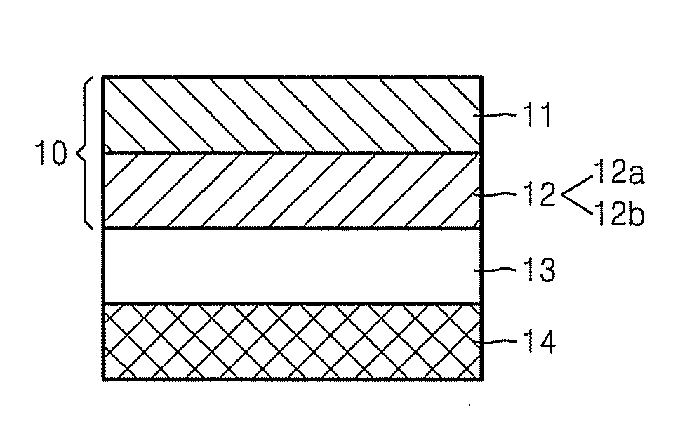
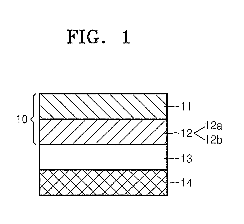
Reduced graphene oxide doped with dopant, thin layer and transparent electrode
a graphene oxide and thin layer technology, applied in the direction of non-metal conductors, sustainable manufacturing/processing, final product manufacturing, etc., can solve the problems of insufficient economic and reproducible process for preparing large-sized graphene sheets, inability to economically and reproducibly prepare single-walled carbon nanotubes, and use of carbon nanotube products. achieve the effect of improving electrical properties
- Summary
- Abstract
- Description
- Claims
- Application Information
AI Technical Summary
Benefits of technology
Problems solved by technology
Method used
Image

Examples
examples 1 to 13
[0053]1 mg of pure graphite (99.999%, -200 mesh, Alfar Aesar, Inc.), 20 ml of fuming nitric acid and 8.5 mg of sodium chloride oxide were mixed at room temperature. When the mixture was stirred for 24 hours, the mixture was washed, filtered and cleaned to prepare a graphene oxide.
Preparation of Film
[0054]2 mg of the graphene oxide was added to 20 ml of deionized (DI) water, the pH of the mixture was adjusted to 7 or higher using NaOH, and the mixture was sonicated for 2 hours. Then, 200 ml of thus formed aqueous solution was sprayed on a 5 cm×5 cm polyethylene terephthalate substrate using spay coating. The substrate was immersed in a 50 mM NaBH4 solution for 2.5 days to reduce the graphene oxide, and thus a reduced graphene oxide was obtained. The reduced graphene oxide was doped with dopants listed in Table 1 below.
[0055]A 20 mM dopant solution was loaded on a film, and after 30 seconds, spin coating was performed at 2000 rpm for 60 seconds.
[0056...
example 14
[0059]Preparation of Solar Cell
[0060]A paste of titanium oxide particles having a particle size of 5 to 25 nm was coated on a transparent electrode prepared according to Example 1 to an area of 1 cm2, and the resultant was calcined at a low temperature (at 150° C. or less) to prepare a porous titanium oxide layer having a thickness of about 15 μm. Then, dye adsorbing treatment was performed in a 0.3 mM solution of Ru(4,4′-dicarboxy-2,2′-bipyridine)2(NCS)2 dissolved in ethanol for 12 hours or longer at room temperature. Then, the porous titanium oxide layer on which the dye was adsorbed was washed using ethanol and dried at room temperature to prepare a photocathode.
[0061]A Pt reduction electrode was deposited on a transparent electrode according to Example 1 by sputtering and a microhole was formed using a drill having a diameter of 0.75 mm for injection of an electrolyte to prepare an opposing electrode.
[0062]The photocathode and the opposing electrode were combined by placing a 60...
example 15
[0063]Preparation of Organic Light Emitting Device
[0064]An electrode pattern was formed on a transparent electrode according to Example 1, and washed. Poly(3,4-ethylenedioxythiophene) (PEDOT) was coated on the washed transparent electrode to a thickness of 50 nm, and the resultant was baked at 120° C. for about 5 minutes to prepare a hole injection layer.
[0065]A green 223 polymer was spin coated on the hole injection layer, and baked at 100° C. for 1 hour. A solvent was completely removed in a vacuum oven to form an emitting layer with a thickness of 80 nm.
[0066]Then, Alq3 was vacuum deposited on the polymer emitting layer using a vacuum depositor at 1.0 Å / sec while maintaining the vacuum level at 4×10⁻⁶ torr or less to form an electron transport layer with a thickness of 30 nm. LiF was vacuum deposited at 0.1 Å / sec to form an electron injection layer with a thickness of 5 nm.
[0067]Then, Al was vacuum deposited at 10 Å / sec to form a cathode with a thickness of 200 nm, and the result...
PUM
| Property | Measurement | Unit |
|---|---|---|
| thickness | aaaaa | aaaaa |
| thickness | aaaaa | aaaaa |
| thickness | aaaaa | aaaaa |
Abstract
Description
Claims
Application Information