

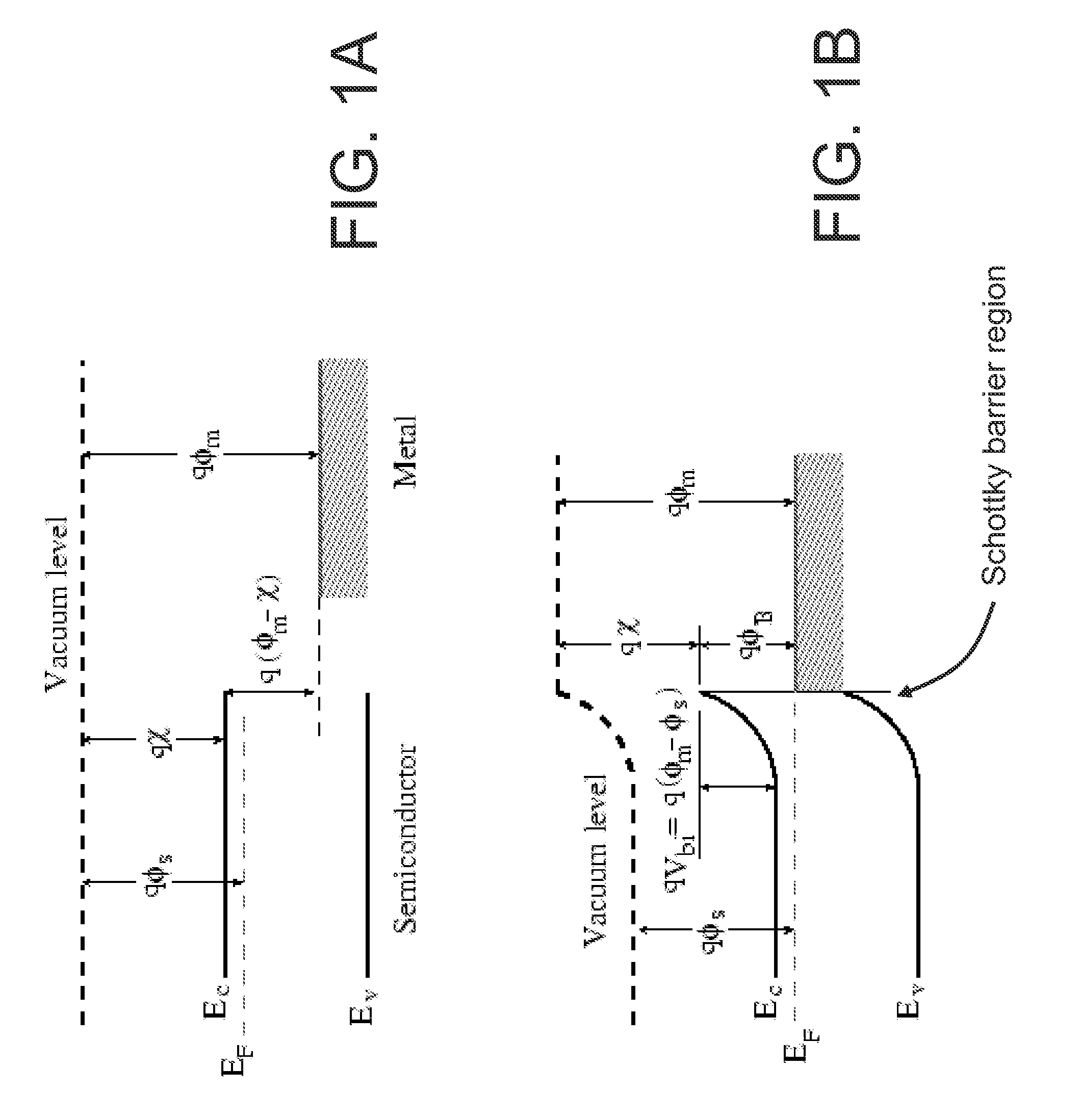
Electronics including graphene-based hybrid structures
a hybrid structure and graphene technology, applied in the direction of carbon-silicon compound conductors, electrical devices, semiconductor devices, etc., can solve the problems of schottky barrier preventing the flow of charge carriers between the semiconductor and the metal, and achieve high thermal conductivity, high intrinsic carrier mobility, and high young's module
- Summary
- Abstract
- Description
- Claims
- Application Information
AI Technical Summary
Benefits of technology
Problems solved by technology
Method used
Image


Examples
example 2d
[0145 materials herein can include a single-atom-thick or a single-polyhedral-thick layer of materials such that the atomic organization or bond strength can be substantially within the layer. The single-atom or single-polyhedral nature of 2D materials also results in small thickness (normally on the order of nanometers), which can make 2D materials lightweight, bendable, rollable, portable, and potentially foldable.
[0146]Three classes of materials that can be prepared as single-atom or single-polyhedral-thick layer are described.
[0147]The first class of materials that can be reduced to stable single-atom or single-polyhedral layers are layered van der Waals solids. These crystal structures have neutral, single-atom-thick or single-polyhedral-sick layers of atom that are covalently or ionically connected with their neighbors within each layer, whereas different layers are held together via van der Waals bonding along the third axis. Since van der Waals bonding is typically weak (aro...
PUM
 Abstract
Description
Claims
Application Information