
Organic light-emitting display device and method of manufacturing the same

a technology of light-emitting display and organic materials, which is applied in the direction of semiconductor/solid-state device manufacturing, semiconductor devices, electrical apparatus, etc., can solve the problems of reduced yield, increased manufacturing costs, and difficulty in achieving high light-emission efficiency with such a structure, and achieve excellent leakage current properties and reduce driving curren

Inactive Publication Date: 2012-12-27
SAMSUNG DISPLAY CO LTD
View PDF11 Cites 7 Cited by
  • Summary
  • Abstract
  • Description
  • Claims
  • Application Information

AI Technical Summary

Benefits of technology

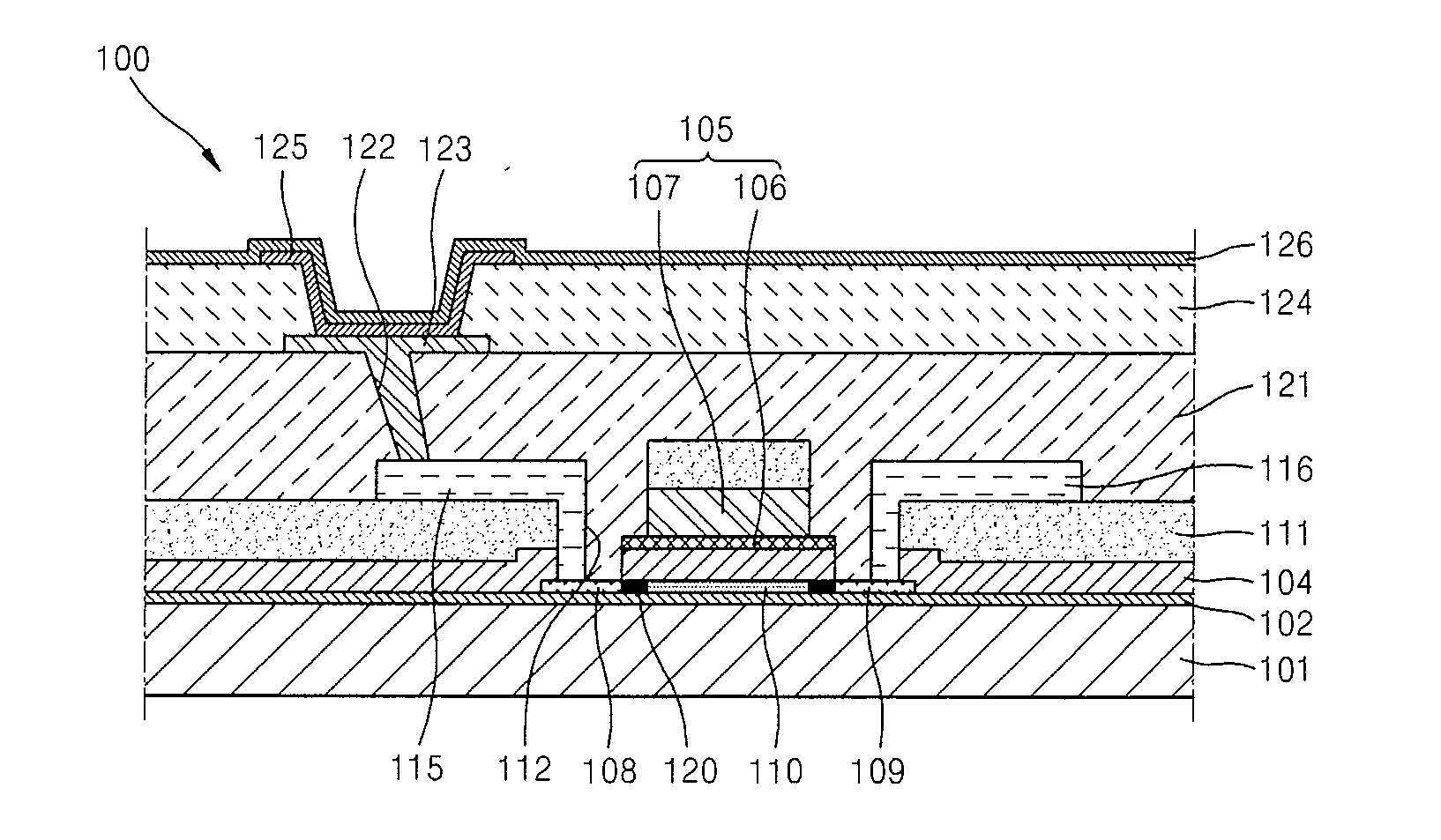
[0012]Aspects of embodiments according to the present invention are directed toward an organic light-emitting display device having reduced driving current and excellent leakage current property by selectively forming a gold overlapped lightly doped drain (GOLDD) structure in a TFT and a method of manufacturing the same.

Problems solved by technology

However, it is difficult to achieve high light-emission efficiency with such a structure, and thus additional intermediate layers, including an electron injection layer, an electron transport layer, a hole transport layer, a hole injection layer, etc., are optionally interposed between the organic emission layer and each of the electrodes.
Thus, yield is reduced and manufacturing costs are increased.

Method used


Image

  • Organic light-emitting display device and method of manufacturing the same
  • Organic light-emitting display device and method of manufacturing the same
  • Organic light-emitting display device and method of manufacturing the same

Examples


Embodiment Construction

[0035]As the present invention allows for various changes and numerous embodiments, particular embodiments will be illustrated in the drawings and described in detail in the written description. However, this is not intended to limit the present invention to particular modes of practice, and it is to be appreciated that all changes, equivalents, and substitutes that do not depart from the spirit and technical scope of the present invention are encompassed in the present invention. In the description of the present invention, certain detailed explanations of related art are omitted when it is deemed that they may unnecessarily obscure the essence of the invention.

[0036]While such terms as “first,”“second,” etc., may be used to describe various components, such components must not be limited to the above terms. The above terms are used only to distinguish one component from another.

[0037]The terms used in the present specification are merely used to describe particular embodiments, an...


PUM


Abstract

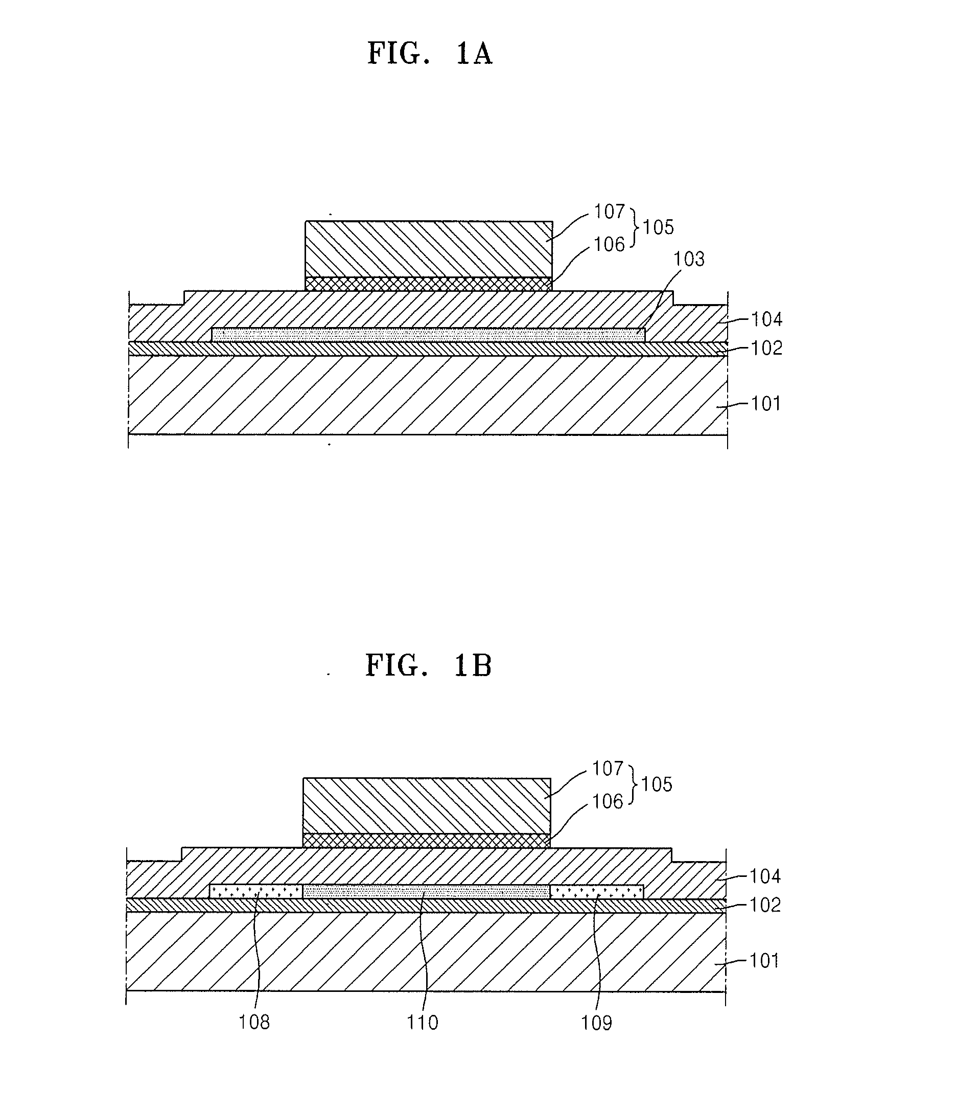
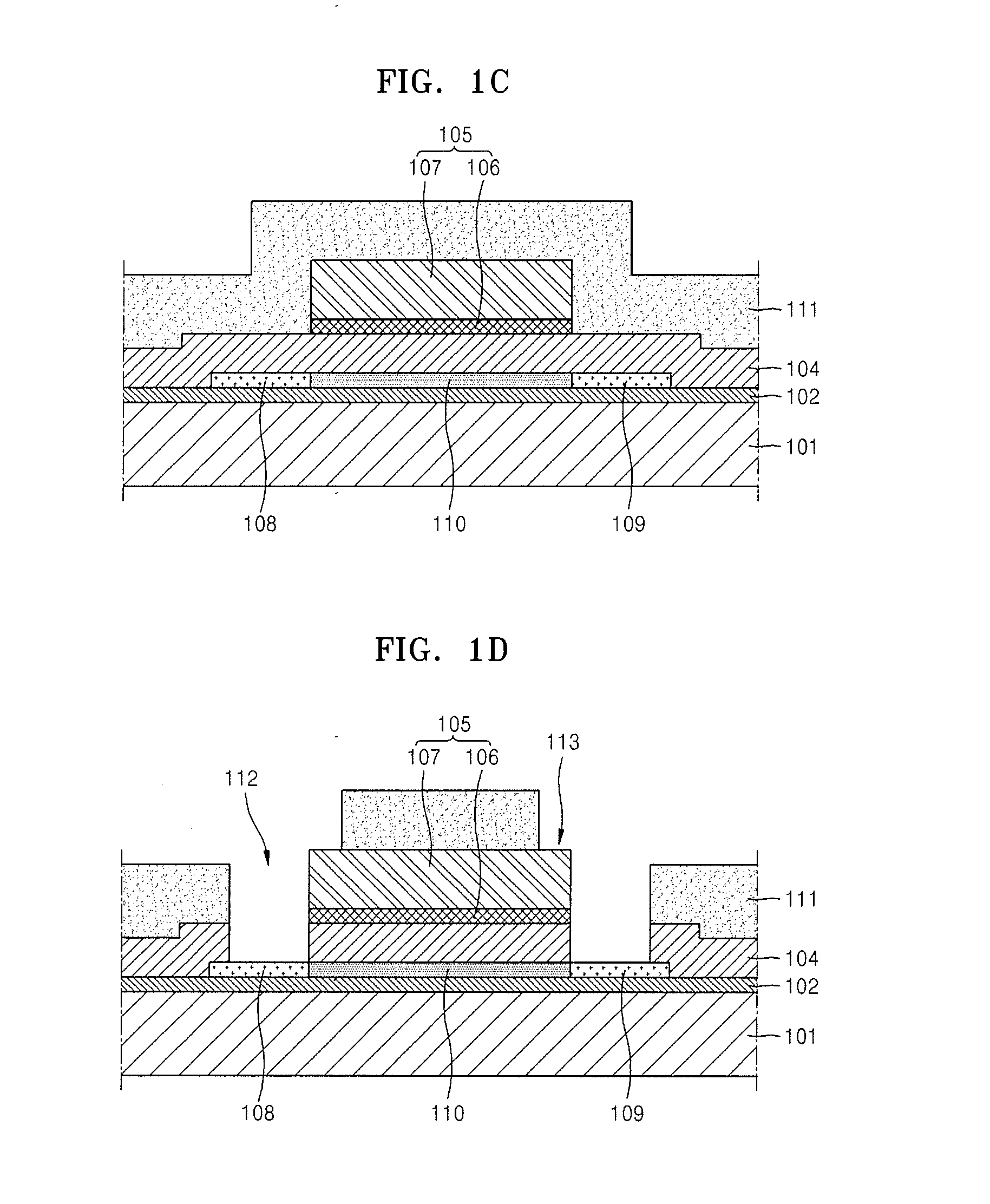
A method of manufacturing an organic light-emitting display device includes forming a gate electrode including a lower gate electrode on a gate insulating layer and an upper gate electrode on the lower gate electrode; forming a source region and a drain region at a semiconductor active layer using the gate electrode as a mask; forming an interlayer insulating layer on a substrate and etching the interlayer insulating layer, resulting in contact holes that expose portions of the source region and the drain region; forming a source / drain electrode raw material on the substrate and etching the source / drain electrode raw material to form a source electrode and a drain electrode; forming a gold overlapped lightly doped drain (GOLDD) structure having a LDD region at the semiconductor active layer by injecting impurity ions; depositing a protective layer on the substrate; and forming a display device on the substrate.

Description

CROSS-REFERENCE TO RELATED PATENT APPLICATION[0001]This application claims priority to and the benefit of Korean Patent Application No. 10-2011-0060230, filed on Jun. 21, 2011, in the Korean Intellectual Property Office, the disclosure of which is incorporated herein in its entirety by reference.BACKGROUND[0002]1. Field[0003]Aspects of embodiments according to the present invention relate to an organic light-emitting display device.[0004]2. Description of Related Art[0005]Organic light-emitting display devices (OLEDs) have been applied in electronic / electric products such as digital cameras, video cameras, camcorders, personal digital assistants (PDAs), smart phones, ultra-thin televisions, ultra-slim laptop computers, tablet personal computers, and flexible display devices.[0006]Organic light-emitting display devices display images in color when holes and electrons, injected respectively from an anode and a cathode, recombine in an organic emission layer. An organic light-emitting ...

Claims


Application Information

Patent Timeline
Patent Type & Authority Applications(United States)
IPC IPC(8): H01L33/62
CPCH01L29/42384H01L27/3262H01L29/78627H10K59/1213H01L29/41733
Inventor PARK, BYOUNG-KEONLEE, TAK-YOUNGSEO, JIN-WOOKLEE, KI-YONGNA, HEUNG-YEOL
Owner SAMSUNG DISPLAY CO LTD
Learn More